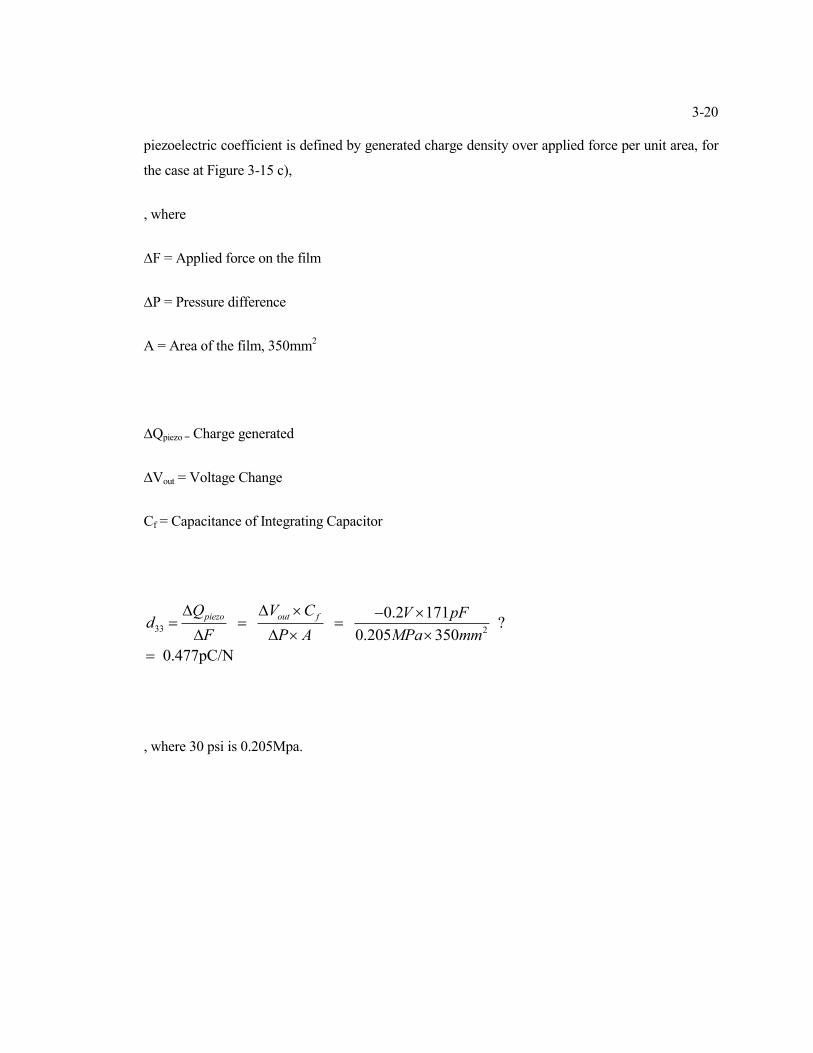
Page 1
Parylene-C as a New Piezoelectric Material
Thesis by
Justin Young-Hyun Kim
In Partial Fulfillment of the Requirements for the degree of
Doctor of Philosophy
CALIFORNIA INSTITUTE OF TECHNOLOGY
Pasadena, California
2013
(Defended 2012.06.22)
Page 2
ii
2013
Justin Young-Hyun Kim
All Rights Reserved
Page 3
iii
To my God,
To my parents and parents in law,
To Sujin, Jaeyeon, Nayeon and Hayeon,
To my friends from CALTECH,
To my brothers and brother in law,
And to Dr. Tai
Page 4
iv
ACKNOWLEDGEMENTS
First, I would like to express my sincere appreciation to Professor Yu-Chong Tai for his academic
and personal guidance and support. His enthusiasm and faith in this project has carried me through
many hard times and has helped me out of many dead ends.
I would also like to thank the staff and students of the Caltech Micromachining Group for their
assistance both inside and outside our lab. I could not have learned so much throughout this Ph.D.
program without the support of Dr. Wen Li, Dr. Mike Liu, Dr. Quoc (Brandon) Quach, Dr. Ray
Huang, Dr. Luca Giacchino, Dr. Jeffrey Lin, Dr. Nick Lo, Dr. Changlin Pang, Dr. Po-Jui (PJ)
Chen, Dr. Jason Shih, Mandheerej (Monty) Nandra, Charles DeBoer, Bo Lu, Penvipha (Yok)
Satsanarukkit, Wendian (Leo) Shi, Han-Chieh (Jay) Chang, Yu (Joy) Zhao, Dongyang (Clark)
Kang, Xiaoxiao (Shell) Zhang, and Austin Cheng. I would like to thank Yang Liu for his
enthusiasm, dedication and perseverance while measuring the piezoelectric coefficient. In addition I
would like to thank Nick Scianmarello for his help in determining the mathematical description of a
circular diaphragm. My appreciation also extends to Trevor Roper, Christine Garske and Tanya
Owen who have done an excellent job in keeping the Caltech Micromachining Lab running
smoothly.
Outside of the lab I would like to thank Taesik Oh for teaching me and helping me to use the XRD
to analyze the crystallinity of PA-C.
I am deeply grateful to my younger brothers Do Hyun Kim and Soo Hyun Kim and my colleague,
Siyang Zheng, for mentorship in the PhD program. Your encouragement, companionship and
devotion have been invaluable to me.
Finally, I would like to express my deepest thanks to my wife Sujin and my kids, Jaeyeon, Nayeon
and Hayeon for always being there for me, and to my parents and my parents in law for all their
sacrifices and support. Their love and patience have made this work possible.
Page 5
v
ABSTRACT
The goal of this thesis is to develop a proper microelectromechanical systems (MEMS) process to
manufacture piezoelectric Parylene-C (PA-C), which is famous for its chemical inertness,
mechanical and thermal properties and electrical insulation. Furthermore, piezoelectric PA-C is
used to build miniature, inexpensive, non-biased piezoelectric microphones.
These piezoelectric PA-C MEMS microphones are to be used in any application where a
conventional piezoelectric and electret microphone can be used, such as in cell phones and hearing
aids. However, they have the advantage of a simplified fabrication process compared with existing
technology. In addition, as a piezoelectric polymer, PA-C has varieties of applications due to its low
dielectric constant, low elastic stiffness, low density, high voltage sensitivity, high temperature
stability and low acoustic and mechanical impedance. Furthermore, PA-C is an FDA approved
biocompatible material and is able to maintain operate at a high temperature.
To accomplish piezoelectric PA-C, a MEMS-compatible poling technology has been developed.
The PA-C film is poled by applying electrical field during heating. The piezoelectric coefficient, -
3.75pC/N, is obtained without film stretching.
The millimeter-scale piezoelectric PA-C microphone is fabricated with an in-plane spiral
arrangement of two electrodes. The dynamic range is from less than 30 dB to above 110 dB SPL
(referenced 20 µPa) and the open-circuit sensitivities are from 0.001 – 0.11 mV/Pa over a frequency
range of 1 - 10 kHz. The total harmonic distortion of the device is less than 20% at 110 dB SPL
and 1 kHz.
Page 6
vi
TABLE OF CONTENTS
ACKNOWLEDGEMENTS .................................................................................................................. iv
ABSTRACT ........................................................................................................................................... v
TABLE OF CONTENTS ...................................................................................................................... vi
LIST OF ILLUSTRATIONS ................................................................................................................. x
LIST OF TABLES ............................................................................................................................. xvii
Chapter 1 .............................................................................................................................................. 1-1
Introduction ................................................................................................................................... 1-1
Motivation .............................................................................................................................. 1-1
Piezoelectric material ............................................................................................................. 1-2
Parylene .................................................................................................................................. 1-5
Micro Electro Mechanical Systems (MEMS) ....................................................................... 1-6
Thesis Outline ............................................................................................................................... 1-8
Chapter 2 .............................................................................................................................................. 2-1
Piezoelectric Microphone Review ............................................................................................... 2-1
Piezoelectricity ....................................................................................................................... 2-1
Definitions of Piezoelectric Coefficients and Directions ..................................................... 2-6
Piezoelectric Polymer ............................................................................................................ 2-8
For being Piezoelectric Polymers. ......................................................................................... 2-9
Mechanism of piezoelectricity in semicrystalline polymers. ............................................. 2-10
Poly-Vinyl DiFluoro (PVDF). ............................................................................................. 2-11
Non-MEMS Piezoelectric Microphone .............................................................................. 2-15
Rochelle Salt transducer ...................................................................................................... 2-15
Piezo-Ceramic Microphone ................................................................................................. 2-16
Piezoelectric Plastic ............................................................................................................. 2-17
MEMS Piezoelectric Microphones ........................................................................................... 2-18
A piezoelectric microphone based on PZT thin films[72] ................................................. 2-19
An AlN MEMS Piezoelectric Microphone for Aeroacoustic Applications[74] ................ 2-22
ZnO on Si integrated acoustic sensor[81] ........................................................................... 2-25
Page 7
vii
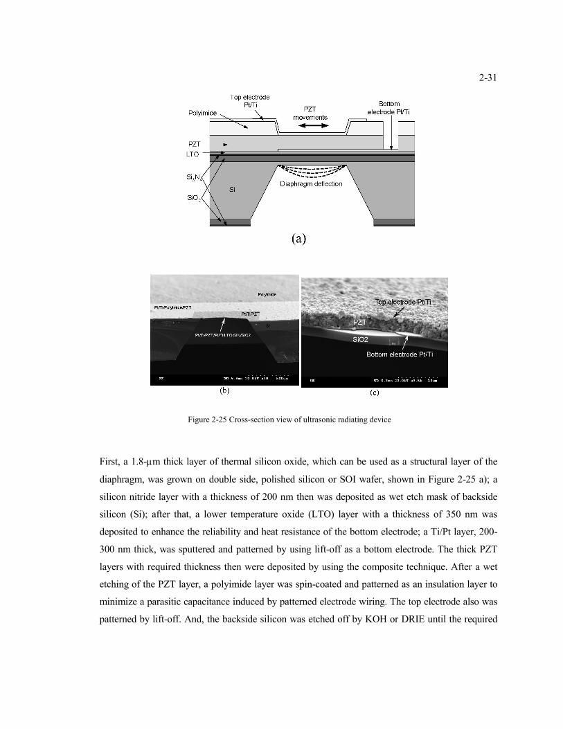
Fabrication and Characterization of Piezoelectric Micromachined Ultrasonic Transducers
with Thick Composite PZT Films[87] ................................................................................ 2-28
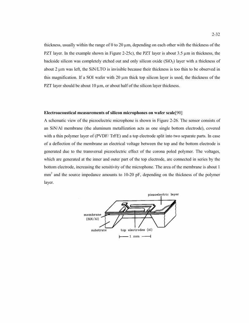
Electroacoustical measurements of silicon microphones on wafer scale[90] .................... 2-32
Microphone based on Polyvinylidene Fluoride (PVDF) micro-pillars and patterned
electrodes[91] ....................................................................................................................... 2-34
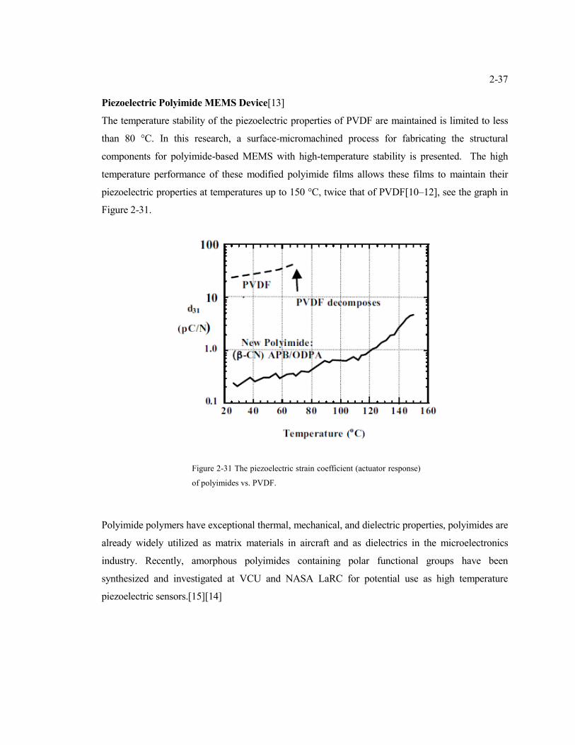
Piezoelectric Polyimide MEMS Device[13] ....................................................................... 2-37
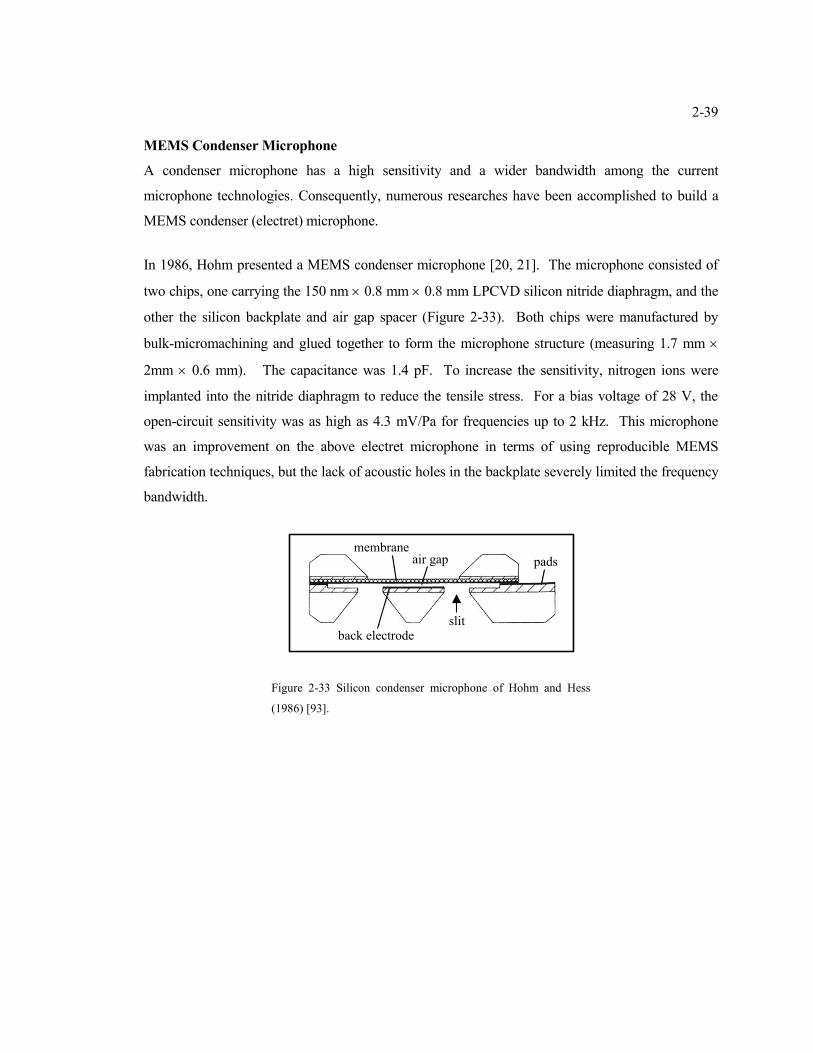
MEMS Condenser Microphone .......................................................................................... 2-39
Summary ..................................................................................................................................... 2-40
Chapter 3 .............................................................................................................................................. 3-1
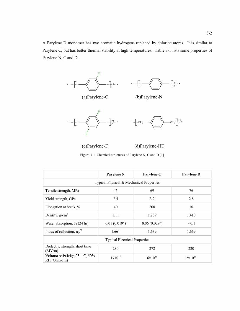
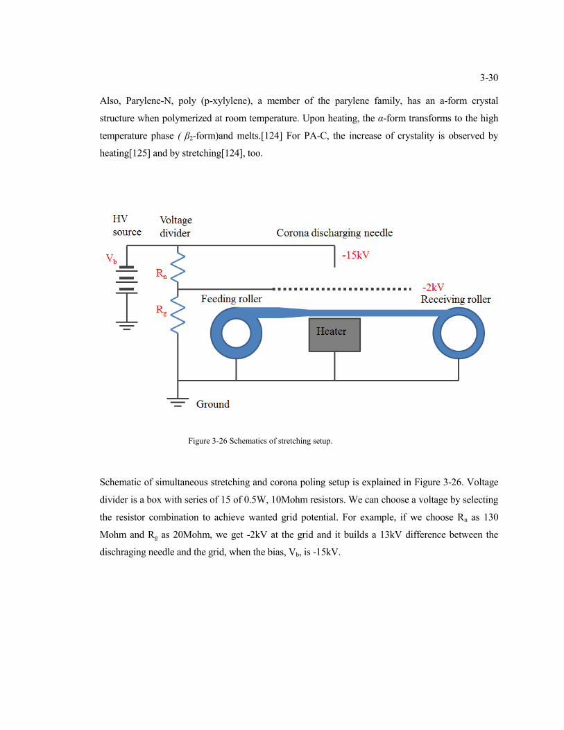
Piezoelectricity of Parylene-C ...................................................................................................... 3-1
Parylene-C .............................................................................................................................. 3-1
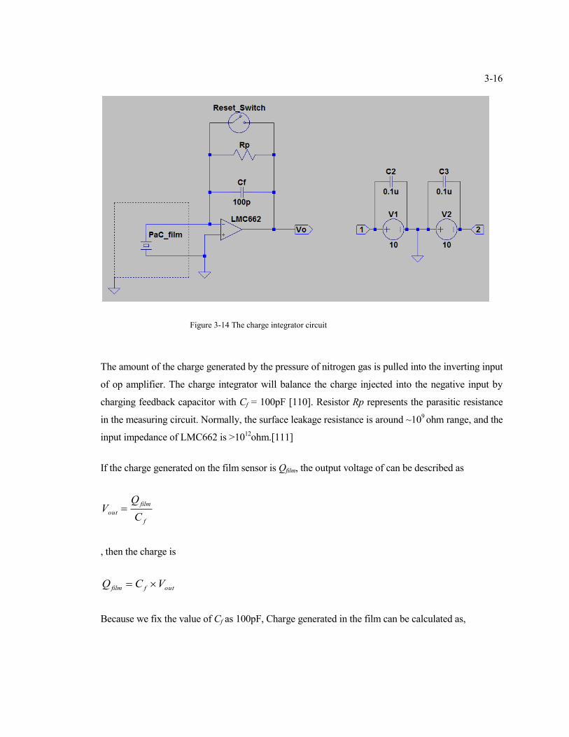
Piezoelectricity of Parylene-C film ....................................................................................... 3-5
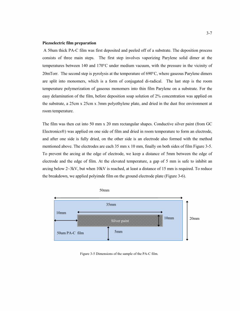
Piezoelectric film preparation ................................................................................................ 3-7
Measuring System ............................................................................................................... 3-11
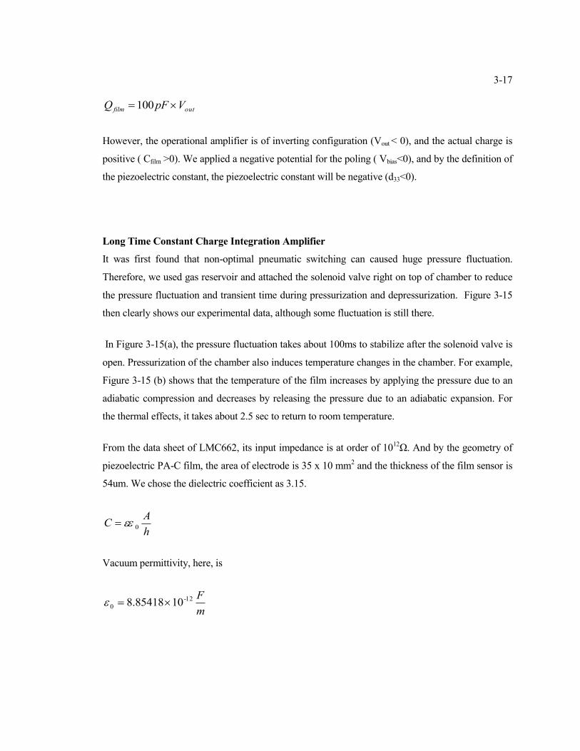
Long Time Constant Charge Integration Amplifier ........................................................... 3-17
d33 Dependence on Poling Condition .................................................................................. 3-21
piezoelectric coefficient over an electrical field........................................................... 3-21
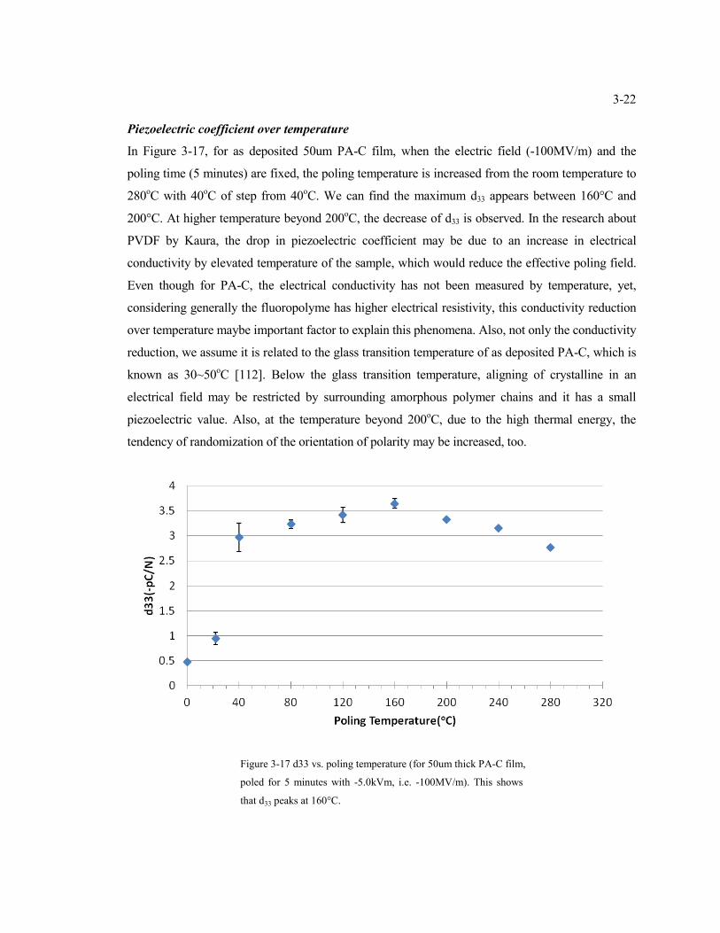
Piezoelectric coefficient over temperature ................................................................... 3-22
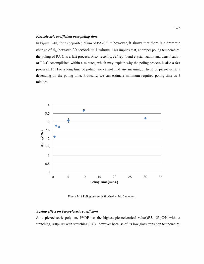
Piezoelectric coefficient over poling time .................................................................... 3-23
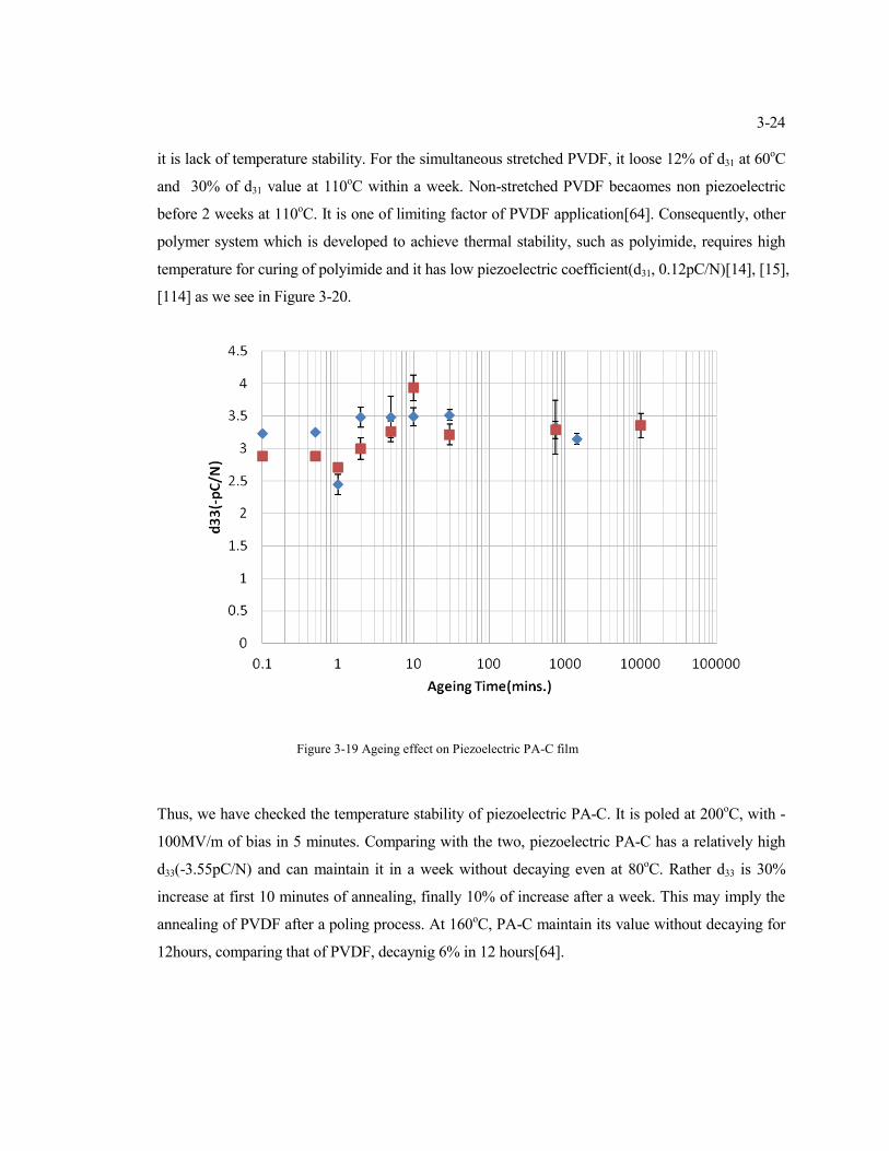
Ageing effect on Piezoelectric coefficient ................................................................... 3-23
Piezoelectric coefficient over pre-annealing time ........................................................ 3-25
Simultaneous Poling and Stretching to Piezoelectric coefficient ................................ 3-26
Summary ..................................................................................................................................... 3-34
Chapter 4 .............................................................................................................................................. 4-1
Microphone Design ...................................................................................................................... 4-1
Design of Microphone ........................................................................................................... 4-1
Model Description and small deflection theory .................................................................... 4-1
Linear Model of Plate with Tension ...................................................................................... 4-3
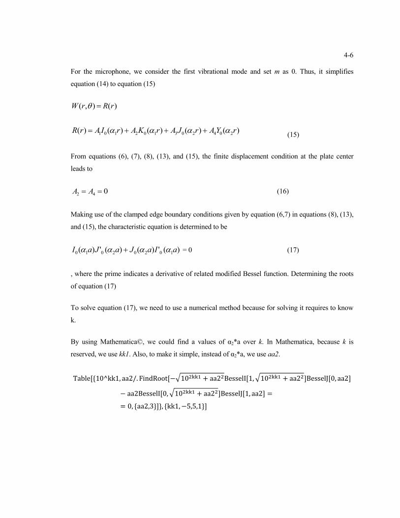
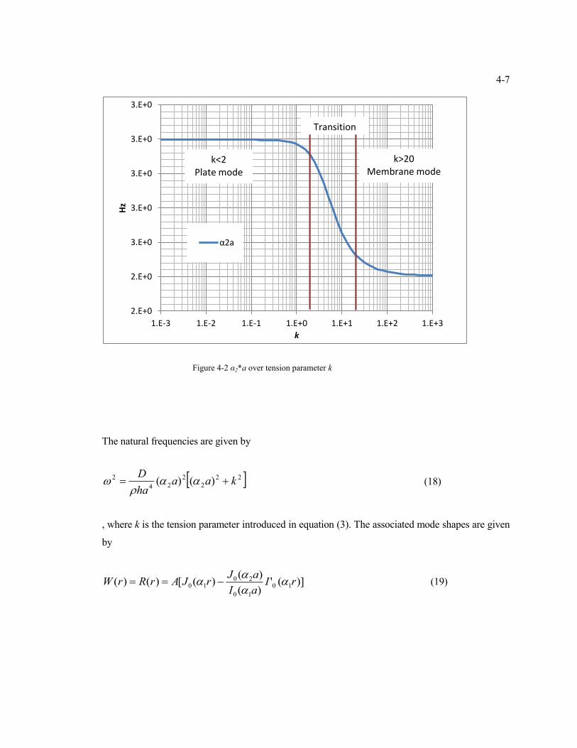
Free Oscillations of Undamped System ................................................................................ 4-4
Transition of Plate-membrane Behavior and Results .......................................................... 4-8
Page 8
viii
Plate Model ( , i.e. ) .................................................................................. 4-8
Membrane Model (D=0) ................................................................................................. 4-8
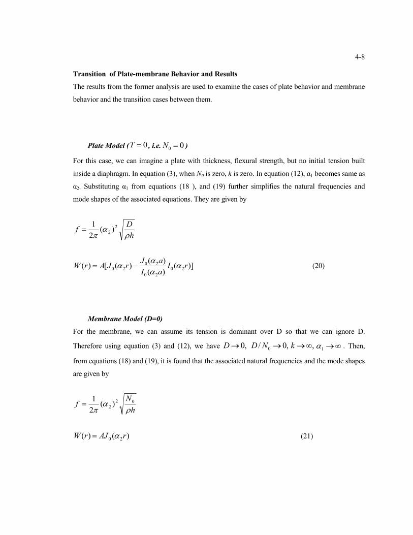
Plate-membrane Transition ................................................................................................... 4-9
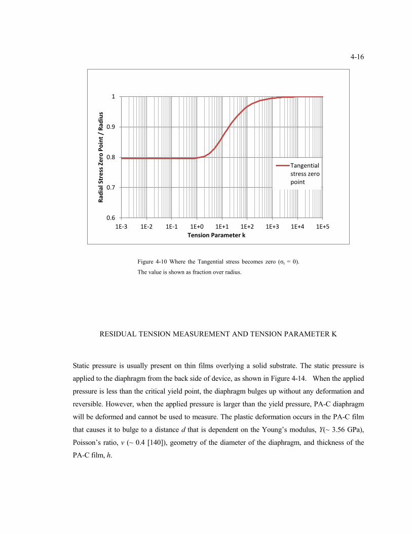
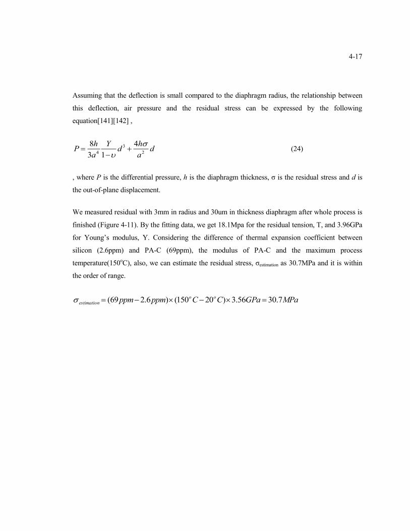
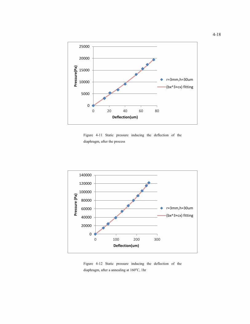
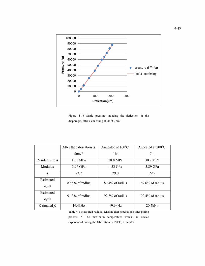
Residual tension measurement and tension parameter k ........................................................... 4-16
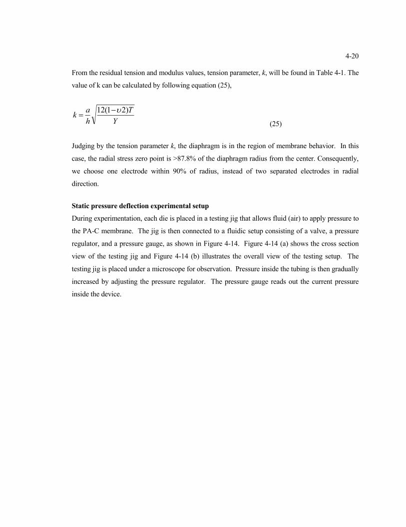
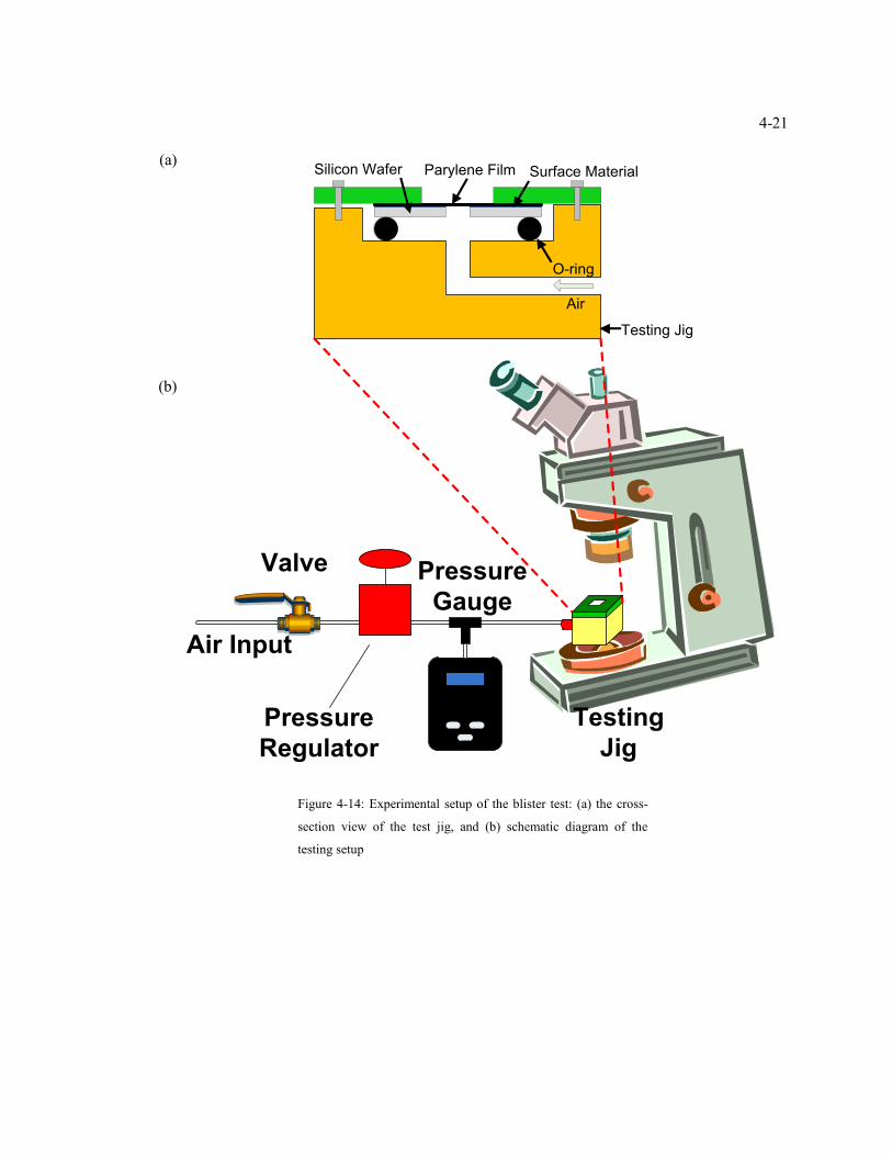
Static pressure deflection experimental setup ..................................................................... 4-20
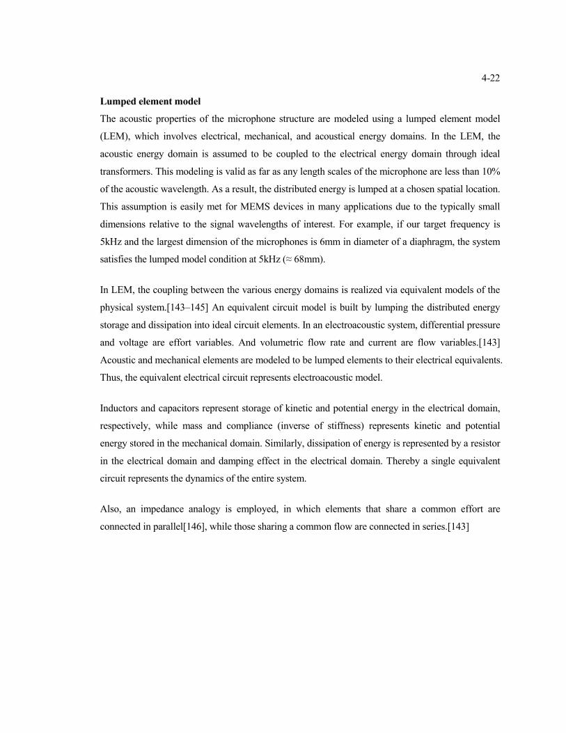
Lumped element model ....................................................................................................... 4-22
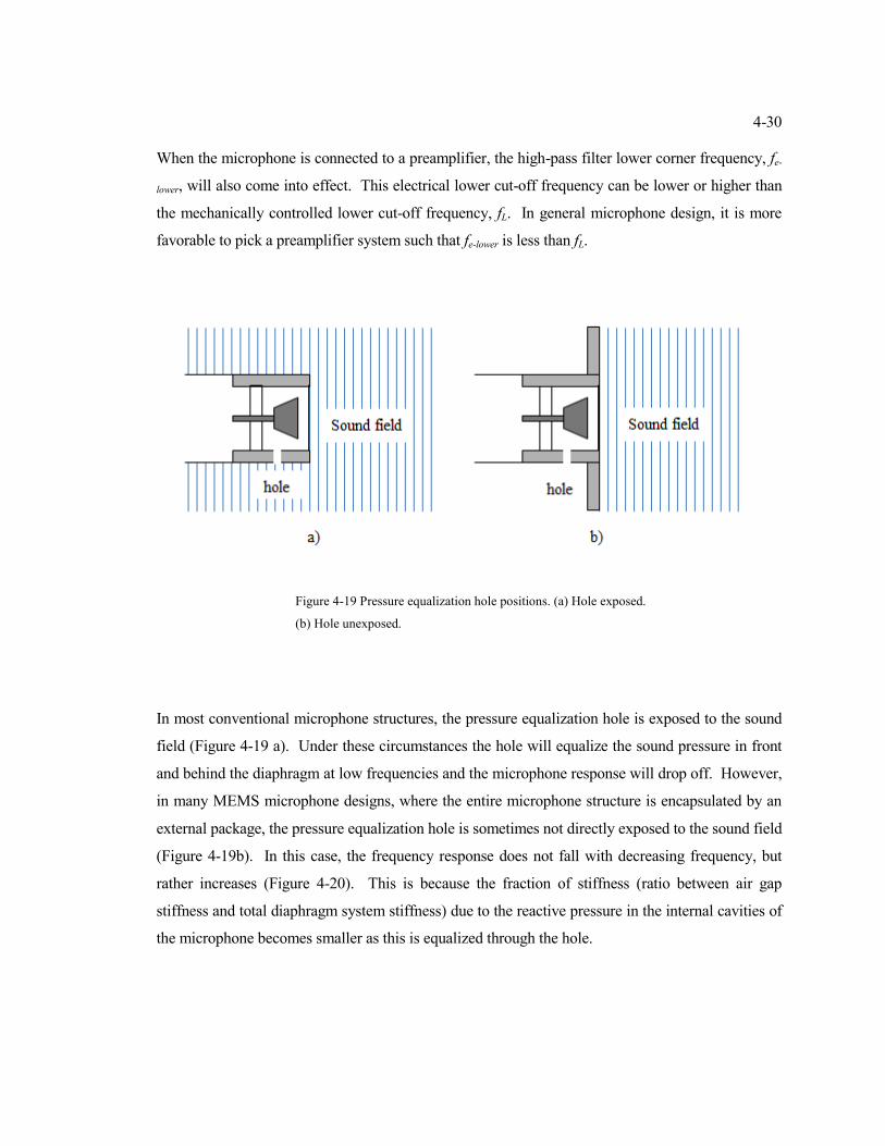
Frequency Response ................................................................................................................... 4-28
Low-Frequency Cut-Off[153] ............................................................................................. 4-29
High-Frequency Cut-Off ..................................................................................................... 4-31
Summary ..................................................................................................................................... 4-34
Chapter 5 .............................................................................................................................................. 5-1
MEMS Piezoelectric Microphones with Piezoelectric Parylene-C Diaphragms ....................... 5-1
Preface .................................................................................................................................... 5-1
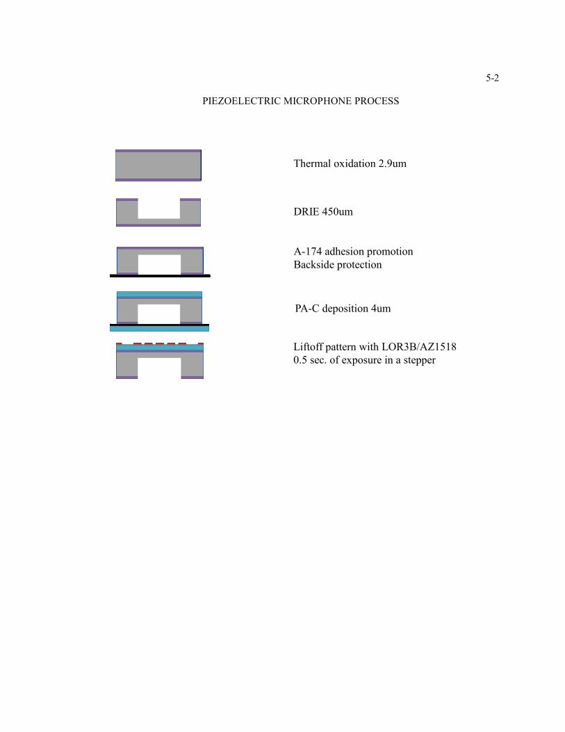
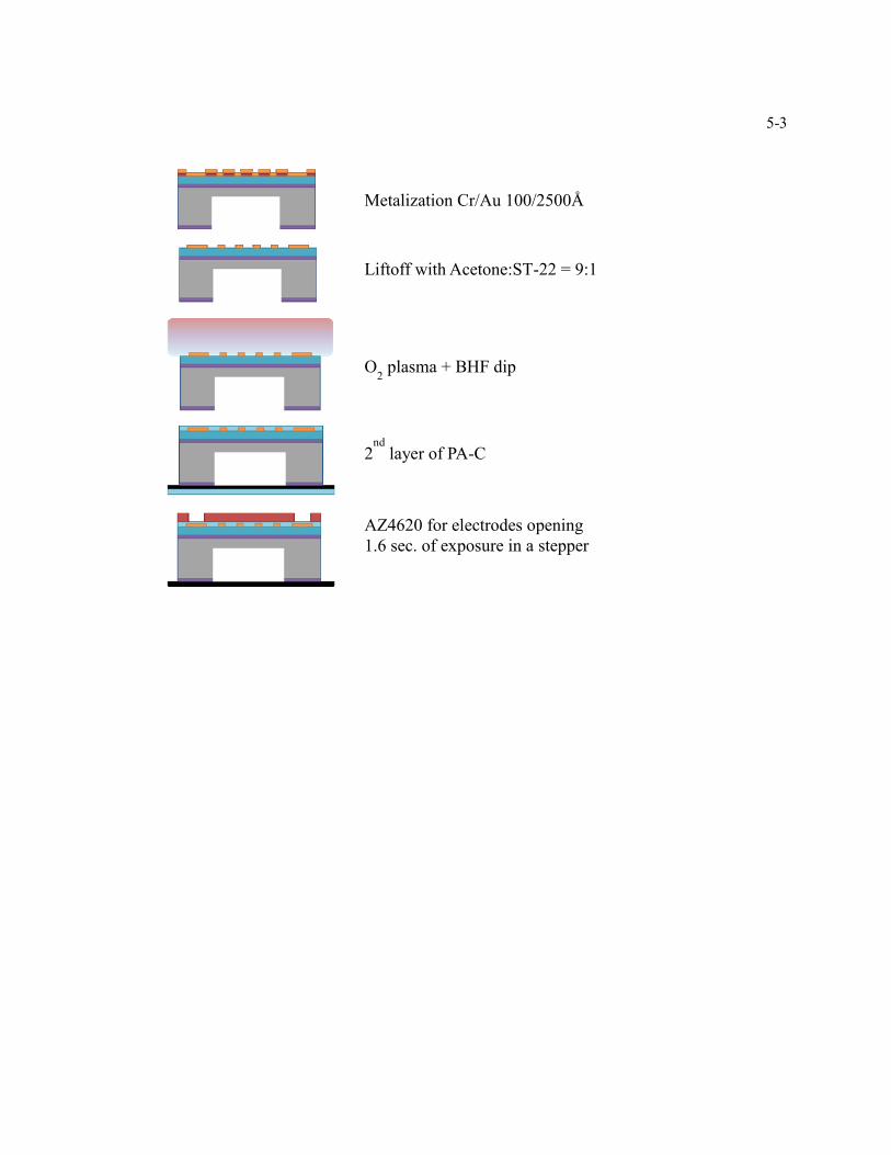
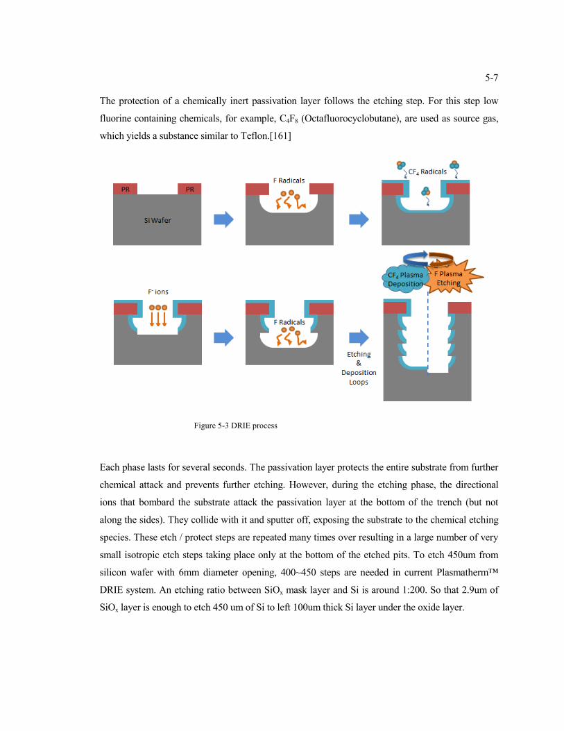
Piezoelectric Microphone Process ............................................................................................... 5-2
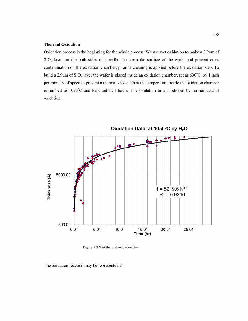
Thermal Oxidation ................................................................................................................. 5-5
DRIE etching for the backside of wafer. ............................................................................... 5-6
A-174 adhesion promotion for PA-C deposit. ...................................................................... 5-8
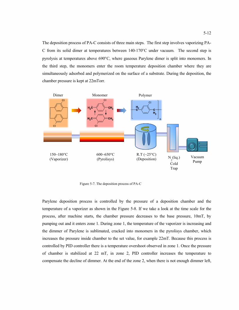
PA-C deposition. .................................................................................................................. 5-11
Liftoff pattern made out of LOR3B and Az1518 ............................................................... 5-14
Metalization ......................................................................................................................... 5-20
Lift off .................................................................................................................................. 5-22
Parylene-Parylene adhesion improvement step .................................................................. 5-24
2nd
PA-C Layer Deposition .................................................................................................. 5-24
Electrodes Opening by O2 Plasma ...................................................................................... 5-24
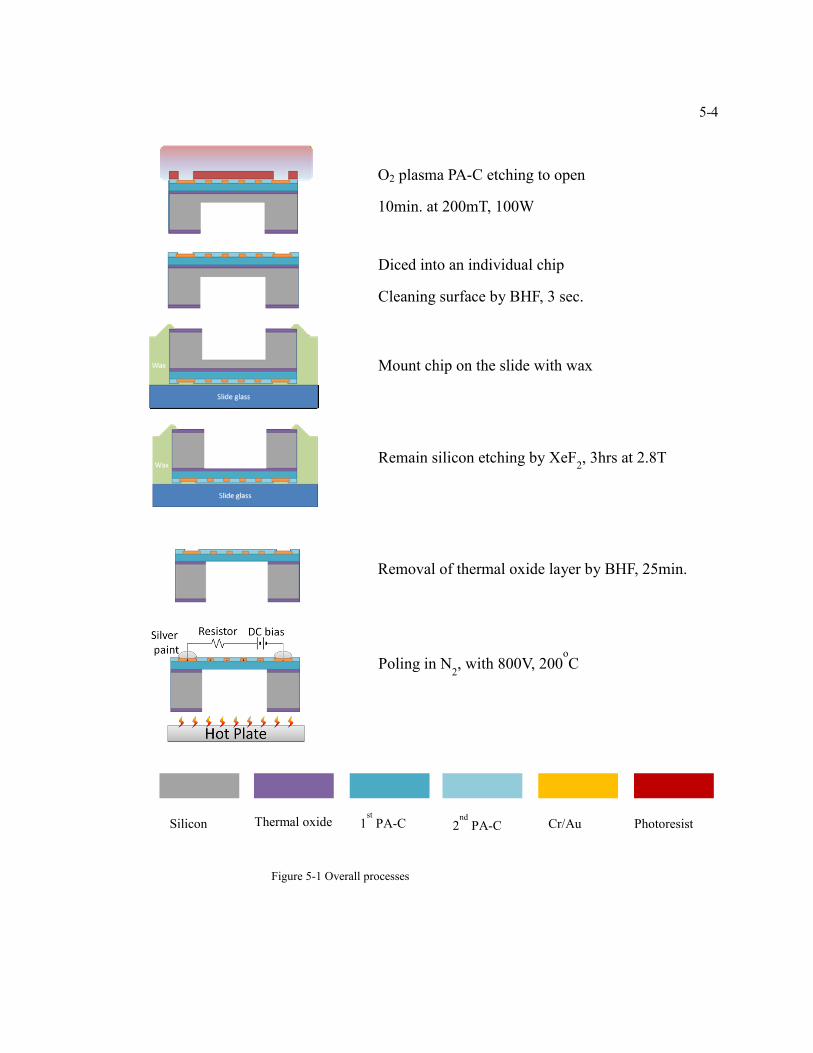
Cleaning surface with BHF and chip mounting .................................................................. 5-26
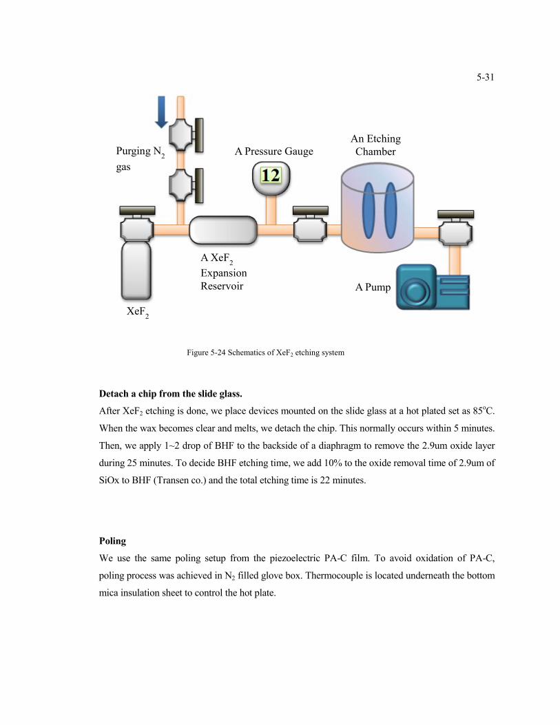
XeF2 etching ......................................................................................................................... 5-26
Detach a chip from the slide glass. ...................................................................................... 5-31
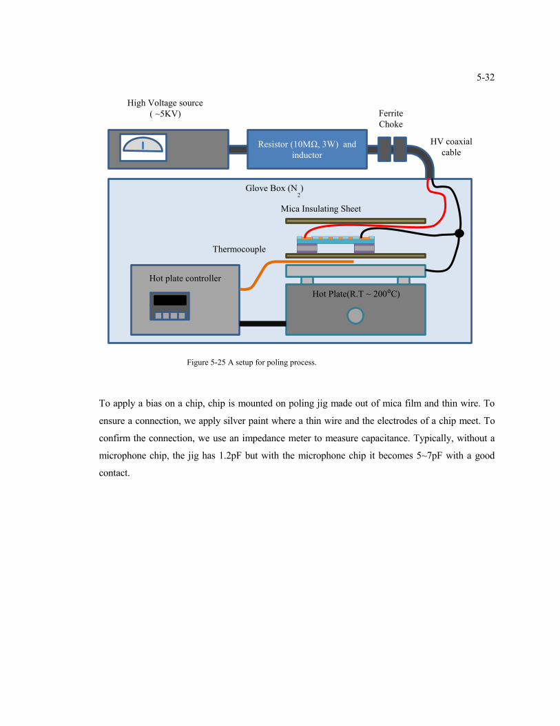
Poling ................................................................................................................................... 5-31
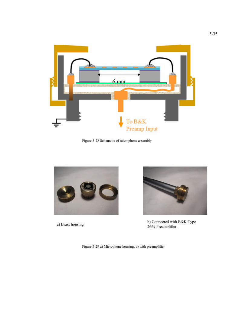
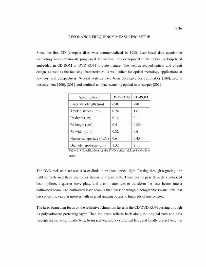
Microphone assembly ................................................................................................................. 5-34
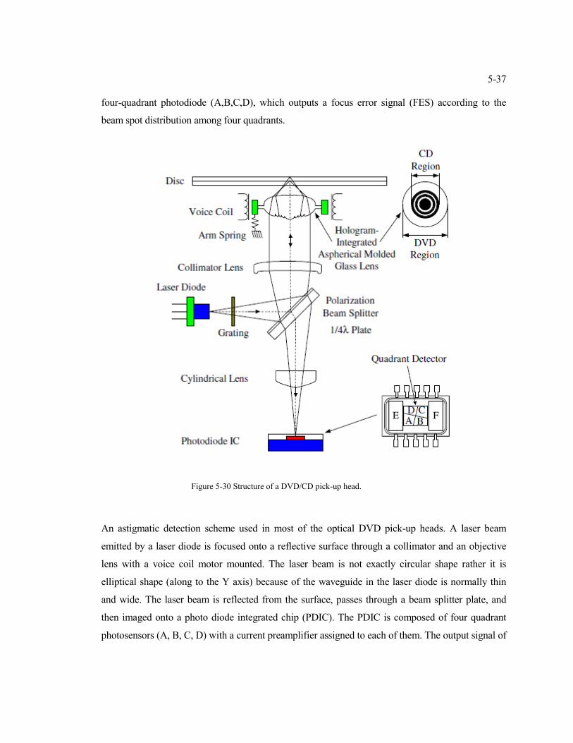
Resonance Frequency Measuring setup ..................................................................................... 5-36
0T 00 N
Page 9
ix
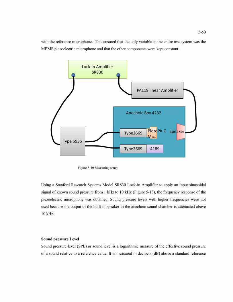
Microphone Measuring Setup .................................................................................................... 5-49
Testing .................................................................................................................................. 5-49
Performance testing ............................................................................................................. 5-49
Sound pressure Level ........................................................................................................... 5-50
Summary ..................................................................................................................................... 5-53
Chapter 6 .............................................................................................................................................. 6-1
Conclusion .................................................................................................................................... 6-1
bibliography .................................................................................................................................. 6-2
Page 10
x
LIST OF ILLUSTRATIONS
Number Page
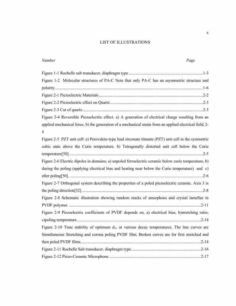
Figure 1-1 Rochelle salt transducer, diaphragm type ......................................................................... 1-3
Figure 1-2 Molecular structures of PA-C Note that only PA-C has an asymmetric structure and
polarity. ................................................................................................................................................ 1-6
Figure 2-1 Piezoelectric Materials ...................................................................................................... 2-2
Figure 2-2 Piezoelectric effect on Quartz ........................................................................................... 2-3
Figure 2-3 Cut of quartz ...................................................................................................................... 2-3
Figure 2-4 Reversible Piezoelectric effect. a) A generation of electrical charge resulting from an
applied mechanical force, b) the generation of a mechanical strain from an applied electrical field. 2-
4
Figure 2-5 PZT unit cell: a) Perovskite-type lead zirconate titanate (PZT) unit cell in the symmetric
cubic state above the Curie temperature. b) Tetragonally distorted unit cell below the Curie
temperature[50]. .................................................................................................................................. 2-5
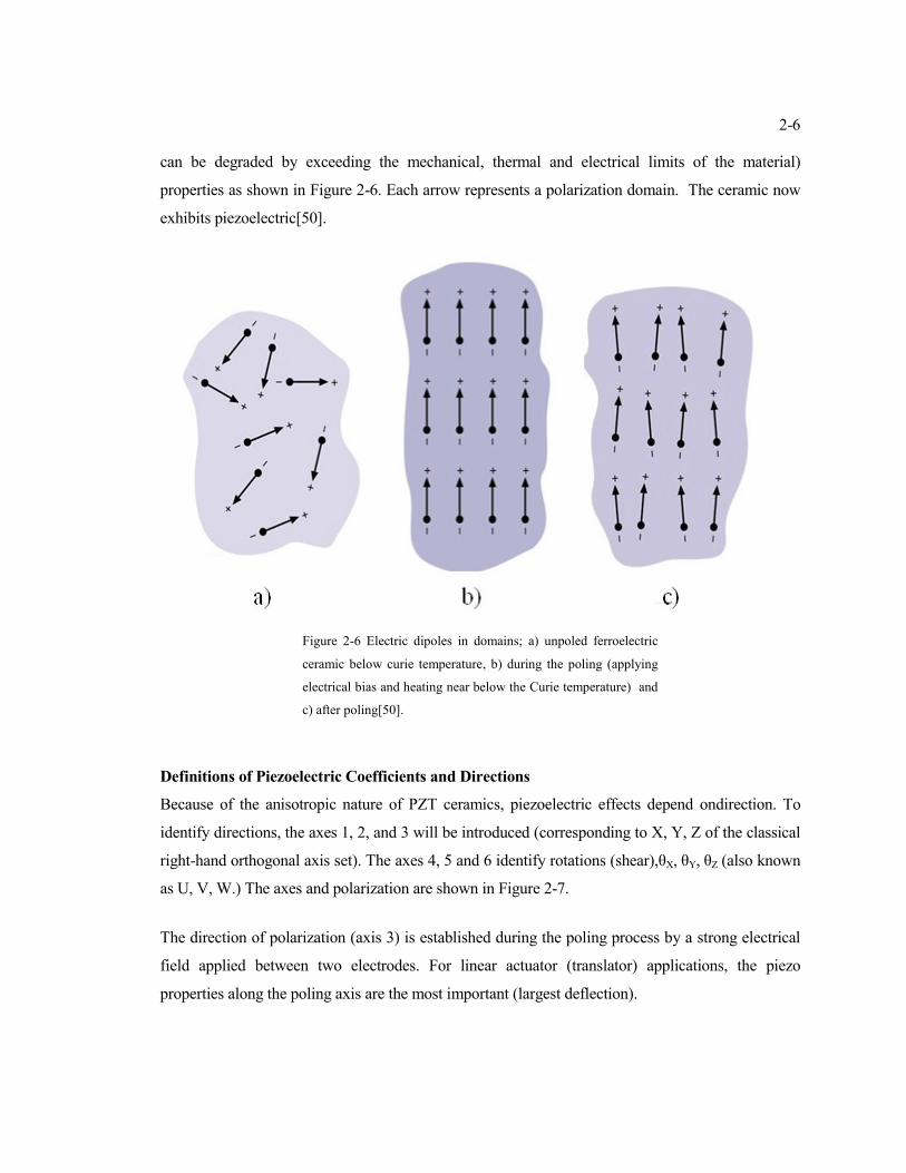
Figure 2-6 Electric dipoles in domains; a) unpoled ferroelectric ceramic below curie temperature, b)
during the poling (applying electrical bias and heating near below the Curie temperature) and c)
after poling[50]. ................................................................................................................................... 2-6
Figure 2-7 Orthogonal system describing the properties of a poled piezoelectric ceramic. Axis 3 is
the poling direction[52]. ...................................................................................................................... 2-8
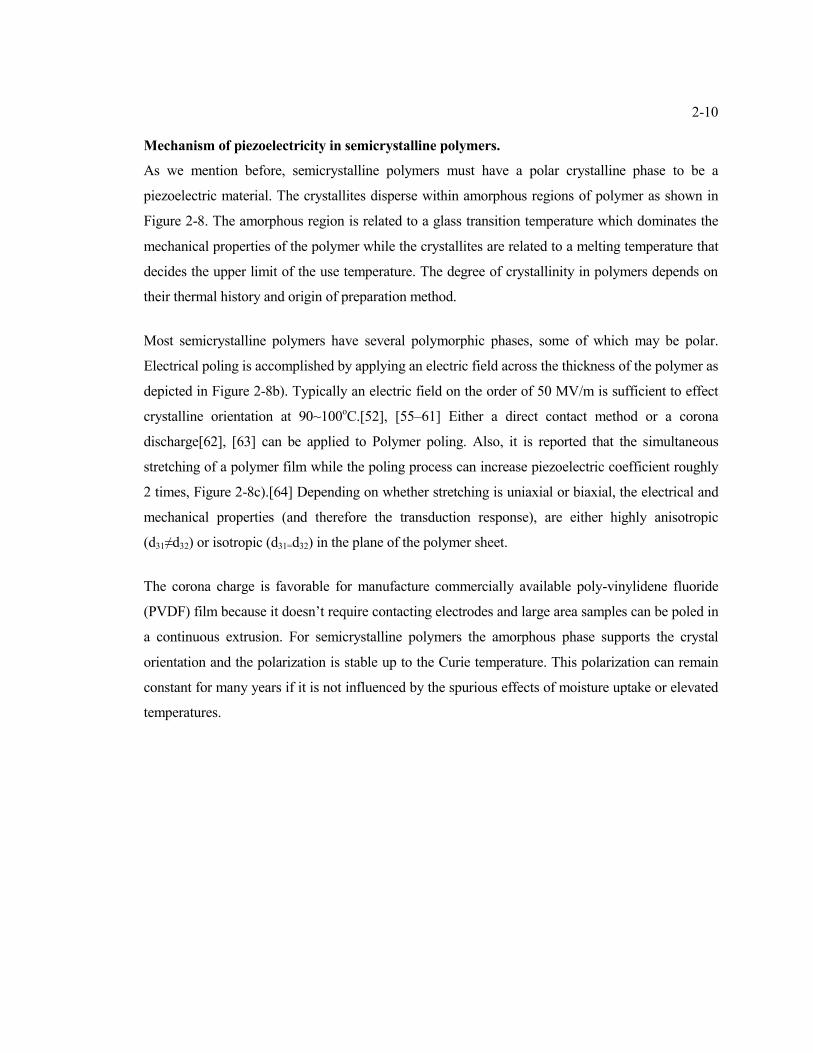
Figure 2-8 Schematic illustration showing random stacks of amorphous and crystal lamellae in
PVDF polymer. ................................................................................................................................. 2-11
Figure 2-9 Piezoelectric coefficients of PVDF depends on, a) electrical bias; b)stretching ratio;
c)poling temperature.......................................................................................................................... 2-14
Figure 2-10 Time stability of optimum d31 at various decay temperatures, The line curves are
Simultaneous Stretching and corona poling PVDF film; Broken curves are for first stretched and
then poled PVDF films. ..................................................................................................................... 2-14
Figure 2-11 Rochelle Salt transducer, diaphragm type. ................................................................... 2-16
Figure 2-12 Piezo-Ceramic Microphone. ......................................................................................... 2-17
Page 11
xi
Figure 2-13 Basic PVDF Transducer................................................................................................ 2-18
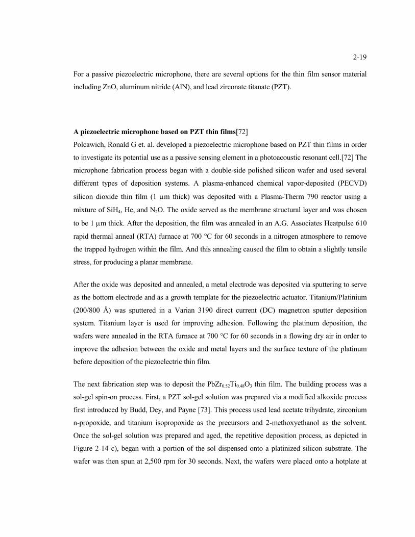
Figure 2-14 Fabrication process flow for creating a PZT membrane microphone: (a) Starting wafer,
(b) sacrificial titanium, (c) Ar ion mill of Ti/Pt/PZT/Pt, (d) PZT wet etch, (e) oxide passivation
deposition, (f) etching of passivation, (g) Ti/Au contact, (h) silicon DRIE, and front view of
released PZT membrane. ................................................................................................................... 2-20
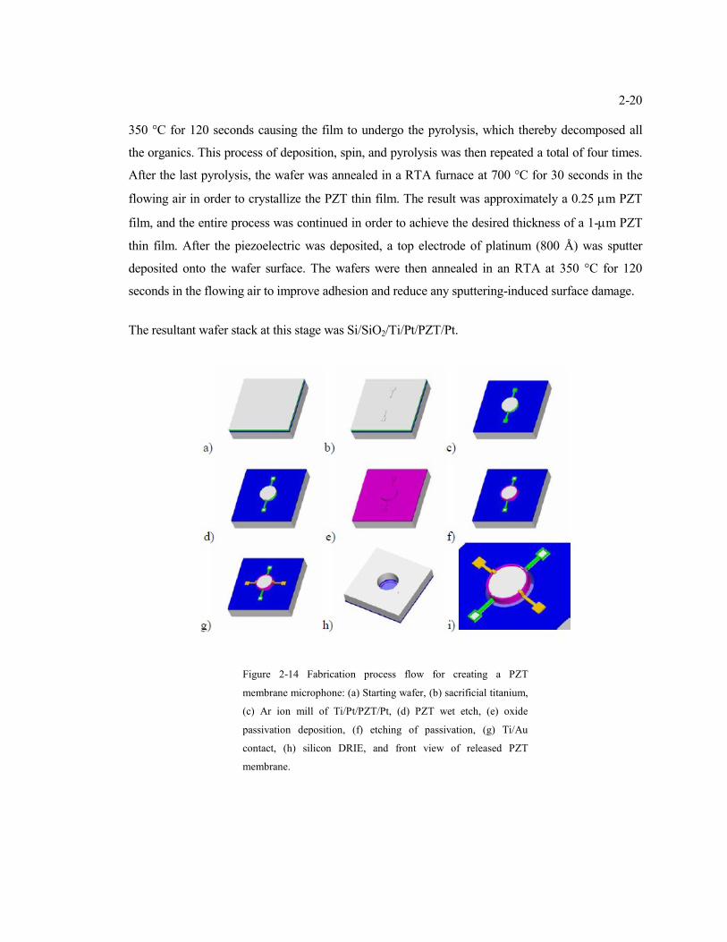
Figure 2-15. Images of the acoustic test chamber used for testing the PZT microphone. (The BNC
mounts provide electrical contact to the packaged microphone whereas the acrylic plate on top
provides a connection for the acoustic tube.) ................................................................................... 2-21
Figure 2-16 Acoustic response of a B&K and a 750-m diameter PZT MEMS microphone with 20%
sensor coverage for B&K Pistonphone 250-Hz tone at 124 dB and ............................................... 2-21
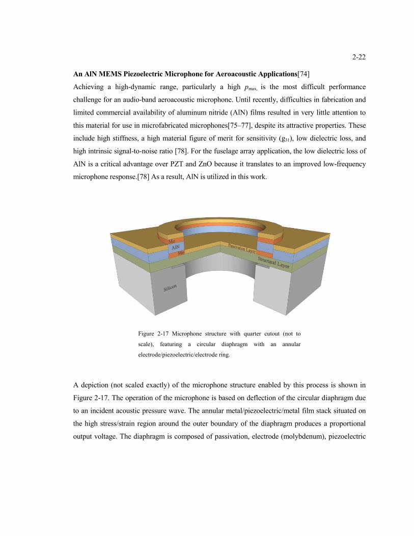
Figure 2-17 Microphone structure with quarter cutout (not to scale), featuring a circular diaphragm
with an annular electrode/piezoelectric/electrode ring. .................................................................... 2-22
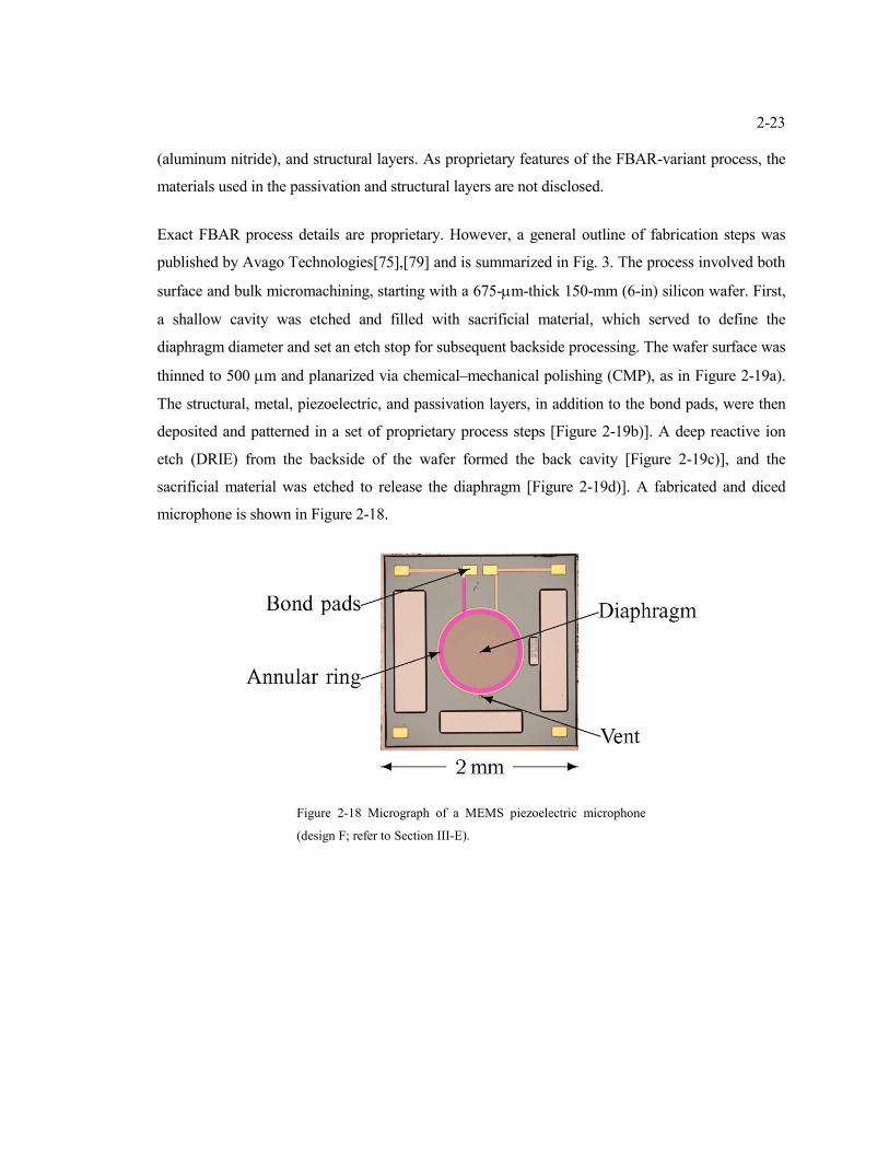
Figure 2-18 Micrograph of a MEMS piezoelectric microphone (design F; refer to Section III-E). ... 2-
23
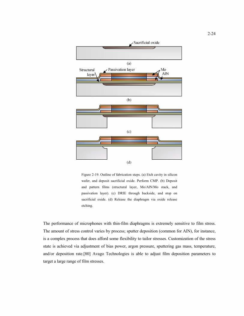
Figure 2-19. Outline of fabrication steps. (a) Etch cavity in silicon wafer, and deposit sacrificial
oxide. Perform CMP. (b) Deposit and pattern films (structural layer, Mo/AlN/Mo stack, and
passivation layer). (c) DRIE through backside, and stop on sacrificial oxide. (d) Release the
diaphragm via oxide release etching. ................................................................................................ 2-24
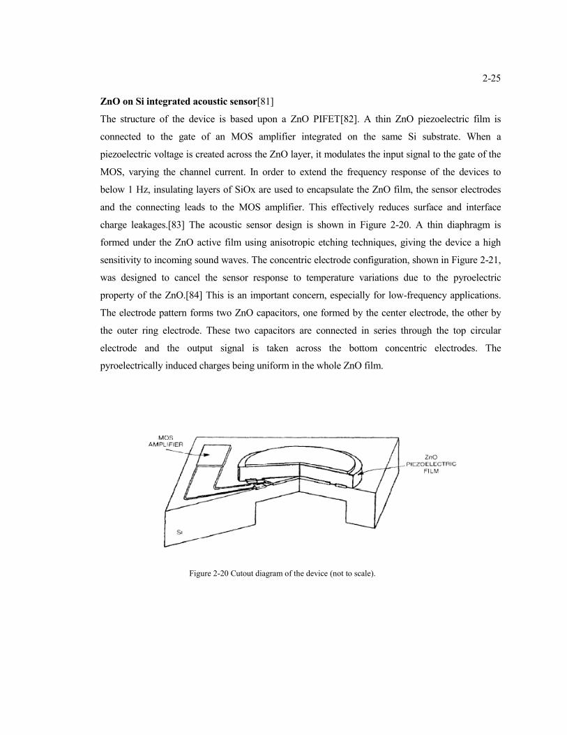
Figure 2-20 Cutout diagram of the device (not to scale). ................................................................. 2-25
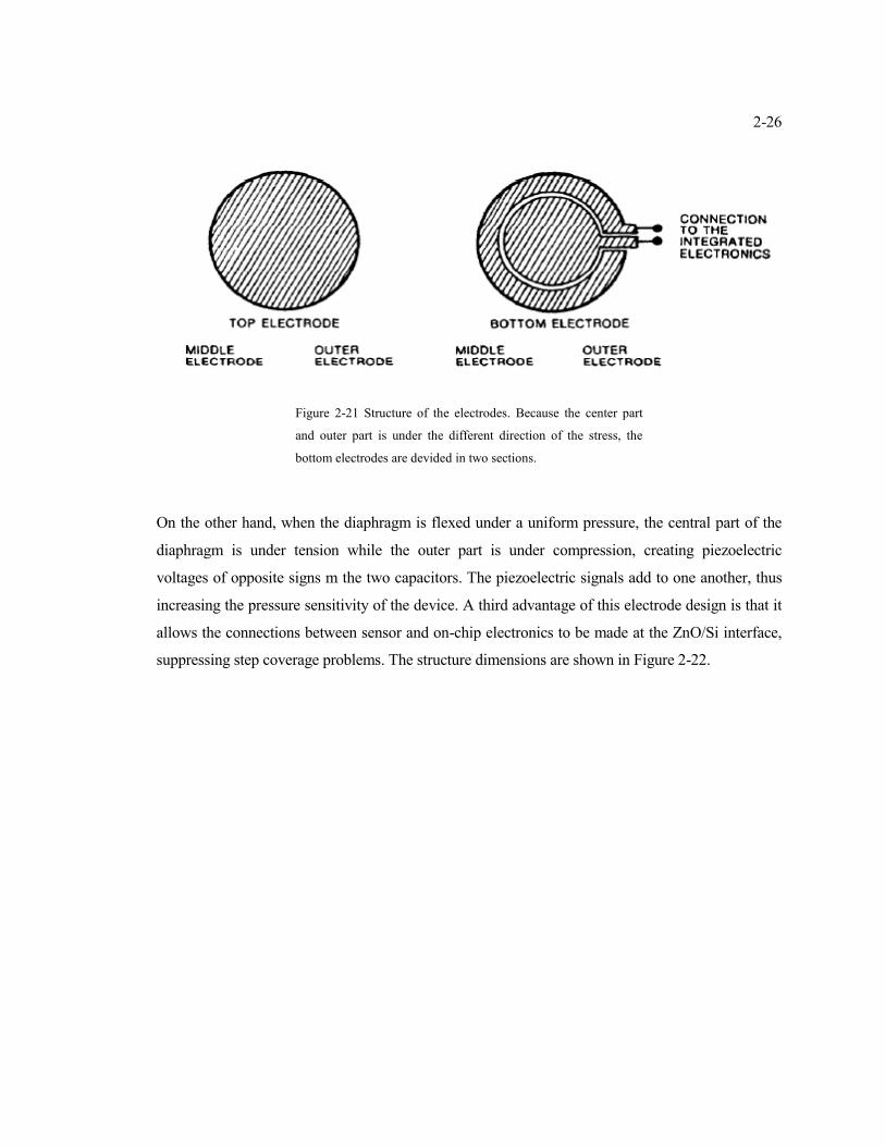
Figure 2-21 Structure of the electrodes. Because the center part and outer part is under the different
direction of the stress, the bottom electrodes are devided in two sections. ..................................... 2-26
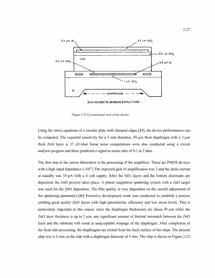
Figure 2-22 Crossectional view of the device. ................................................................................. 2-27
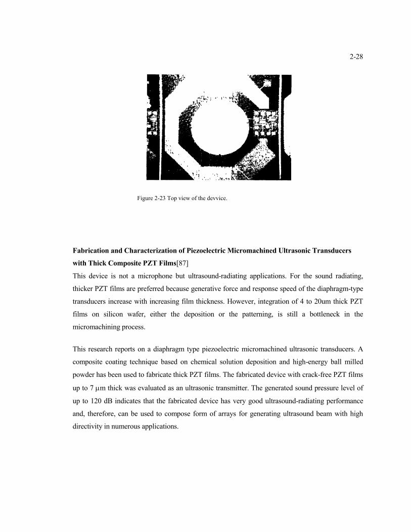
Figure 2-23 Top view of the devvice. ............................................................................................... 2-28
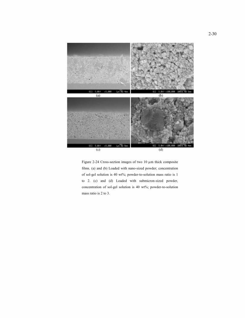
Figure 2-24 Cross-section images of two 10 m thick composite films. (a) and (b) Loaded with
nano-sized powder; concentration of sol-gel solution is 40 wt%; powder-to-solution mass ratio is 1
to 2. (c) and (d) Loaded with submicron-sized powder, concentration of sol-gel solution is 40 wt%;
powder-to-solution mass ratio is 2 to 3. ............................................................................................ 2-30
Figure 2-25 Cross-section view of ultrasonic radiating device ........................................................ 2-31
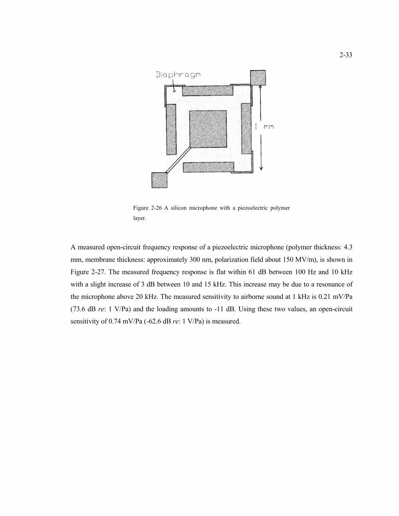
Figure 2-26 A silicon microphone with a piezoelectric polymer layer. .......................................... 2-33
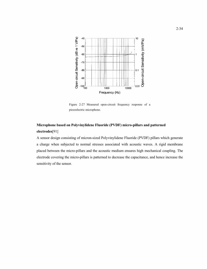
Figure 2-27 Measured open-circuit frequency response of a piezoelectric microphone................. 2-34
Page 12
xii
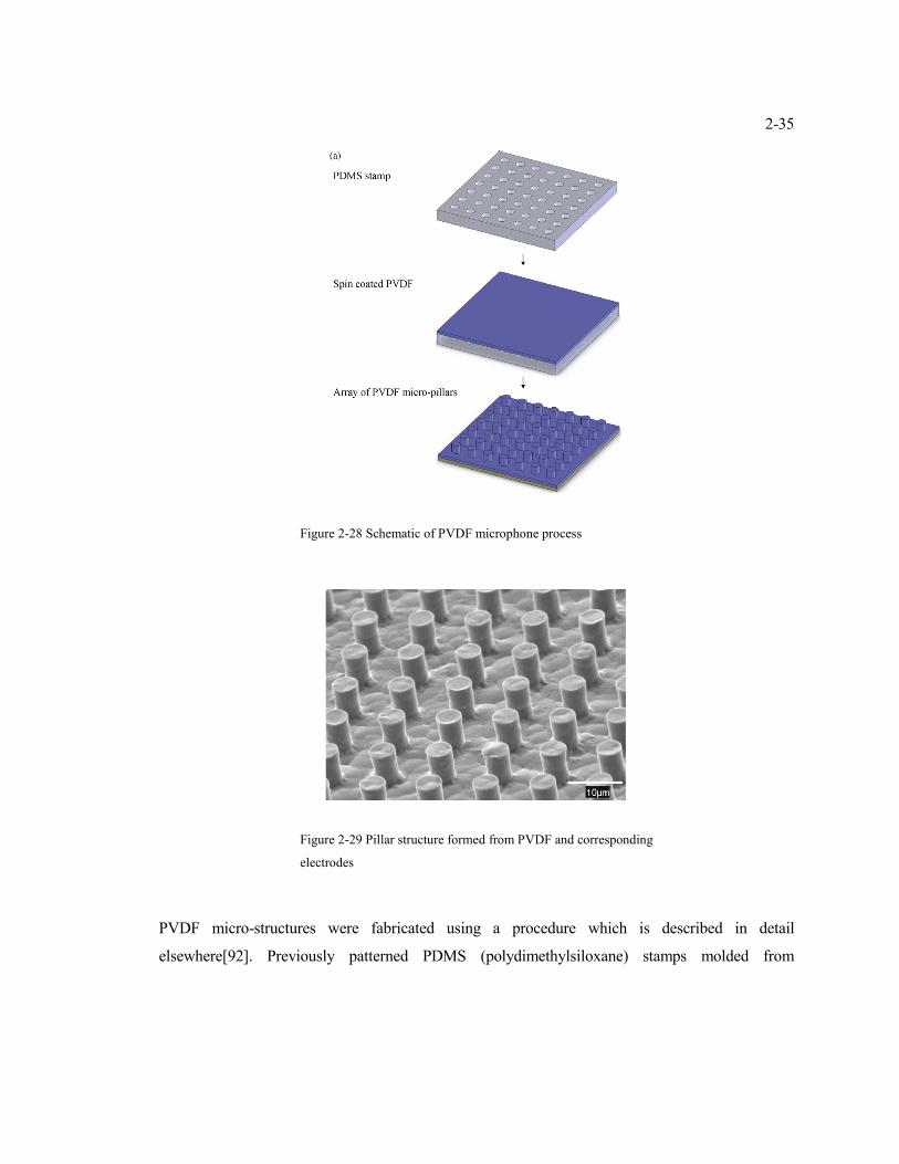
Figure 2-28 Schematic of PVDF microphone process ..................................................................... 2-35
Figure 2-29 Pillar structure formed from PVDF and corresponding electrodes ............................. 2-35
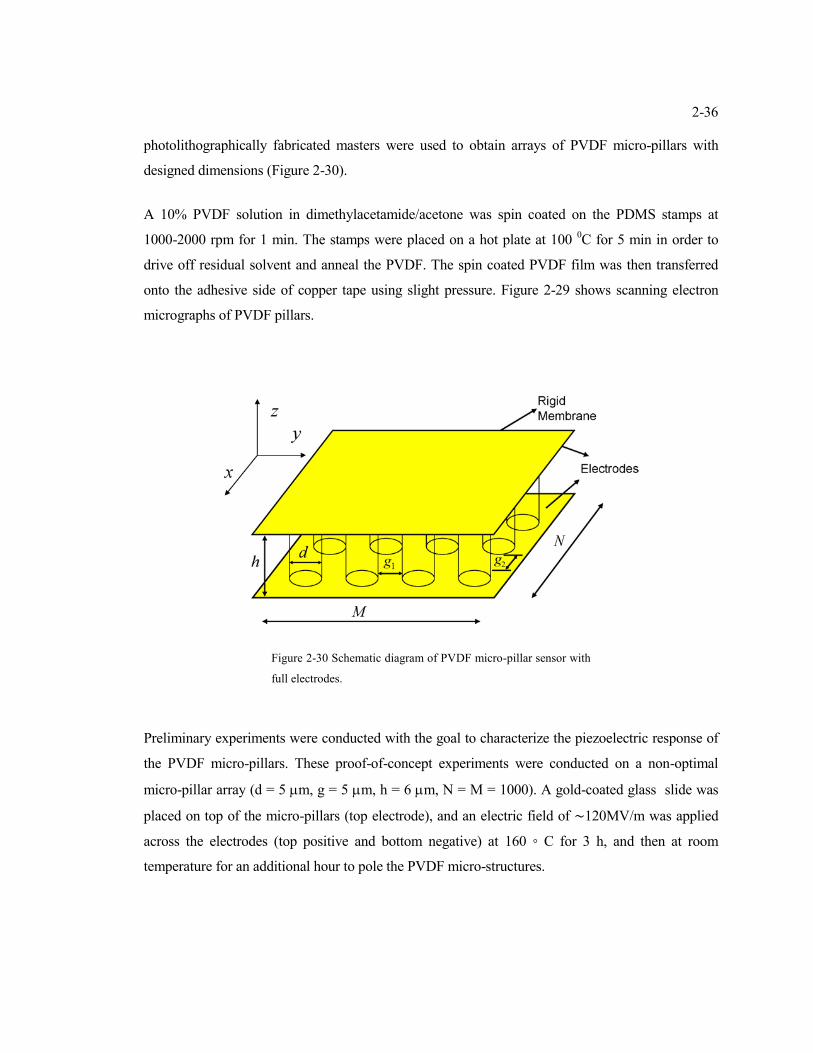
Figure 2-30 Schematic diagram of PVDF micro-pillar sensor with full electrodes. ....................... 2-36
Figure 2-31 The piezoelectric strain coefficient (actuator response) of polyimides vs. PVDF. ..... 2-37
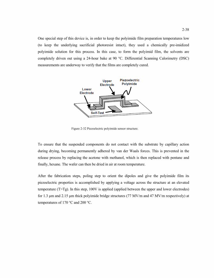
Figure 2-32 Piezoelectric polyimide sensor structure. ..................................................................... 2-38
Figure 2-33 Silicon condenser microphone of Hohm and Hess (1986) [93]. .................................. 2-39
Figure 3-1 Chemical structures of Parylene N, C and D [1]. ............................................................ 3-2
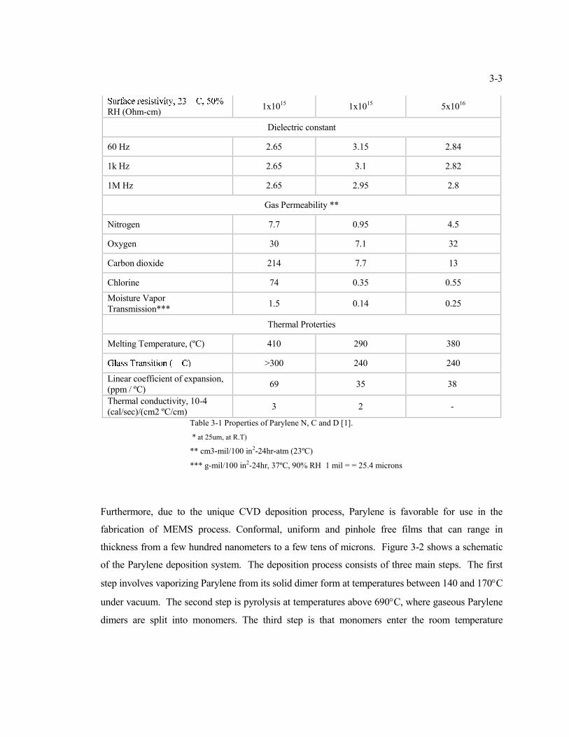
Figure 3-2 Parylene deposition system and the involved chemical processes .................................. 3-4
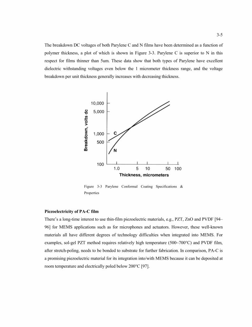
Figure 3-3 Parylene Conformal Coating Specifications & Properties ............................................... 3-5
Figure 3-4 Molecular structures of various type of Parylene. Note that only PA-C has an
asymmetric structure. .......................................................................................................................... 3-6
Figure 3-5 Dimensions of the sample of the PA-C film..................................................................... 3-7
Figure 3-6 Distances from the edges of electrodes of film sample to the edge of bottom ground plate.
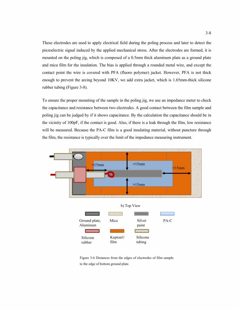
.............................................................................................................................................................. 3-8
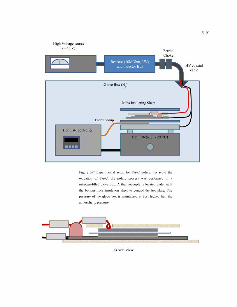
Figure 3-7 Experimental setup for PA-C poling. To avoid the oxidation of PA-C, the poling process
was performed in a nitrogen-filled glove box. A thermocouple is located underneath the bottom
mica insulation sheet to control the hot plate. The pressure of the globe box is maintained at 3psi
higher than the atmospheric pressure. ............................................................................................... 3-10
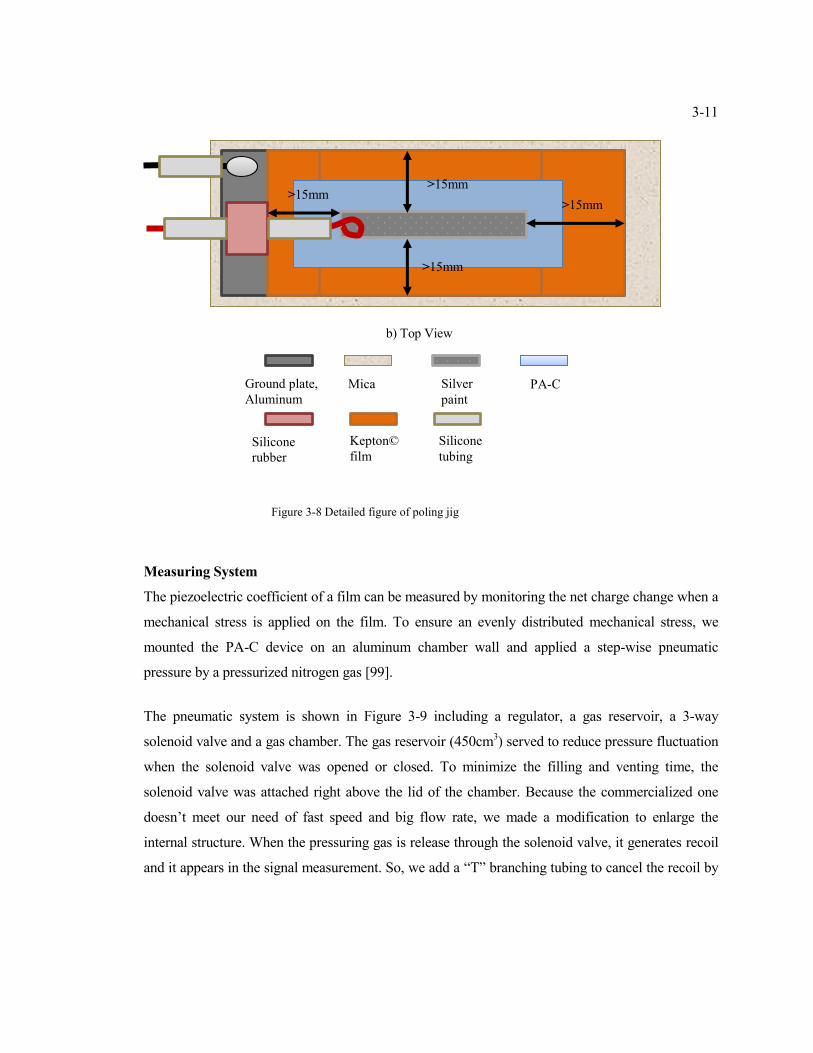
Figure 3-8 Detailed figure of poling jig ............................................................................................ 3-11
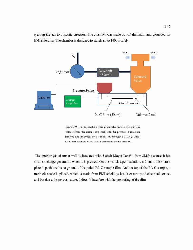
Figure 3-9 The schematic of the pneumatic testing system. The voltage (from the charge amplifier)
and the pressure signals are gathered and analyzed by a control PC through NI DAQ USB-6281.
The solenoid valve is also controlled by the same PC. .................................................................... 3-12
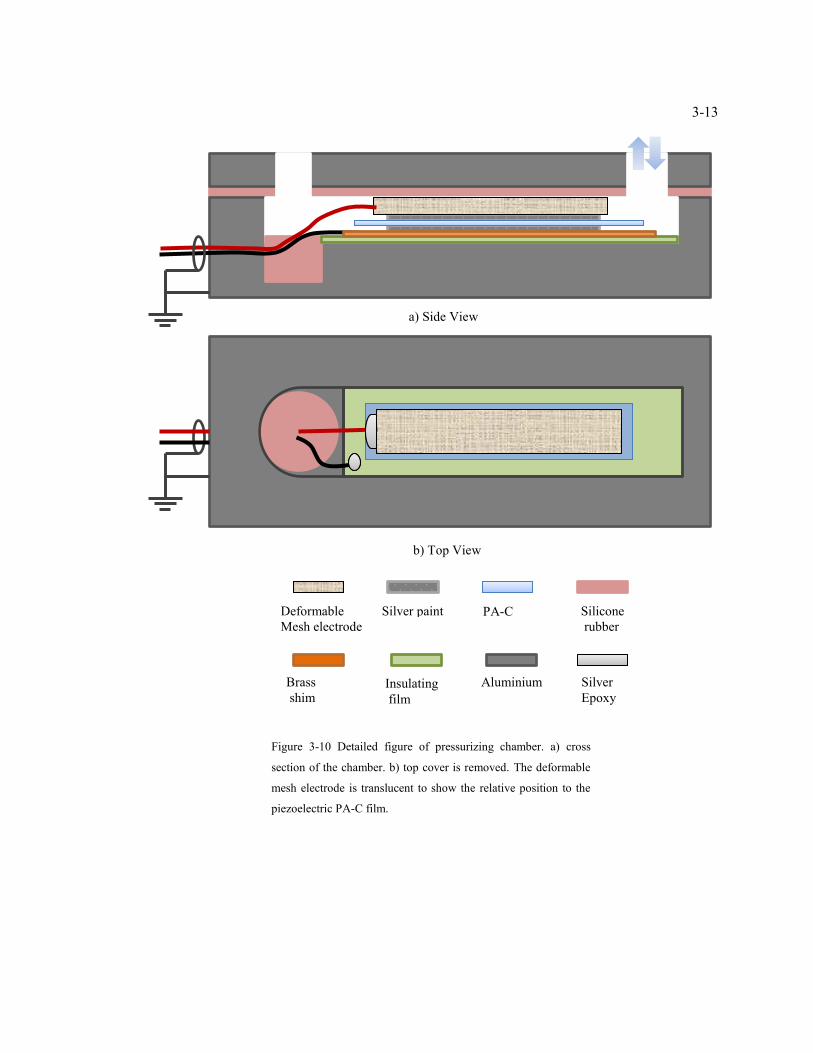
Figure 3-10 Detailed figure of pressurizing chamber. a) cross section of the chamber. b) top cover is
removed. The deformable mesh electrode is translucent to show the relative position to the
piezoelectric PA-C film. .................................................................................................................... 3-13
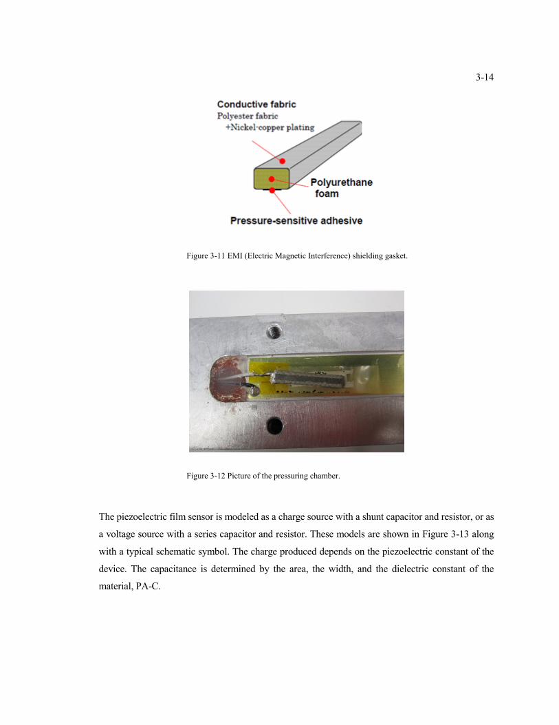
Figure 3-11 EMI (Electric Magnetic Interference) shielding gasket. .............................................. 3-14
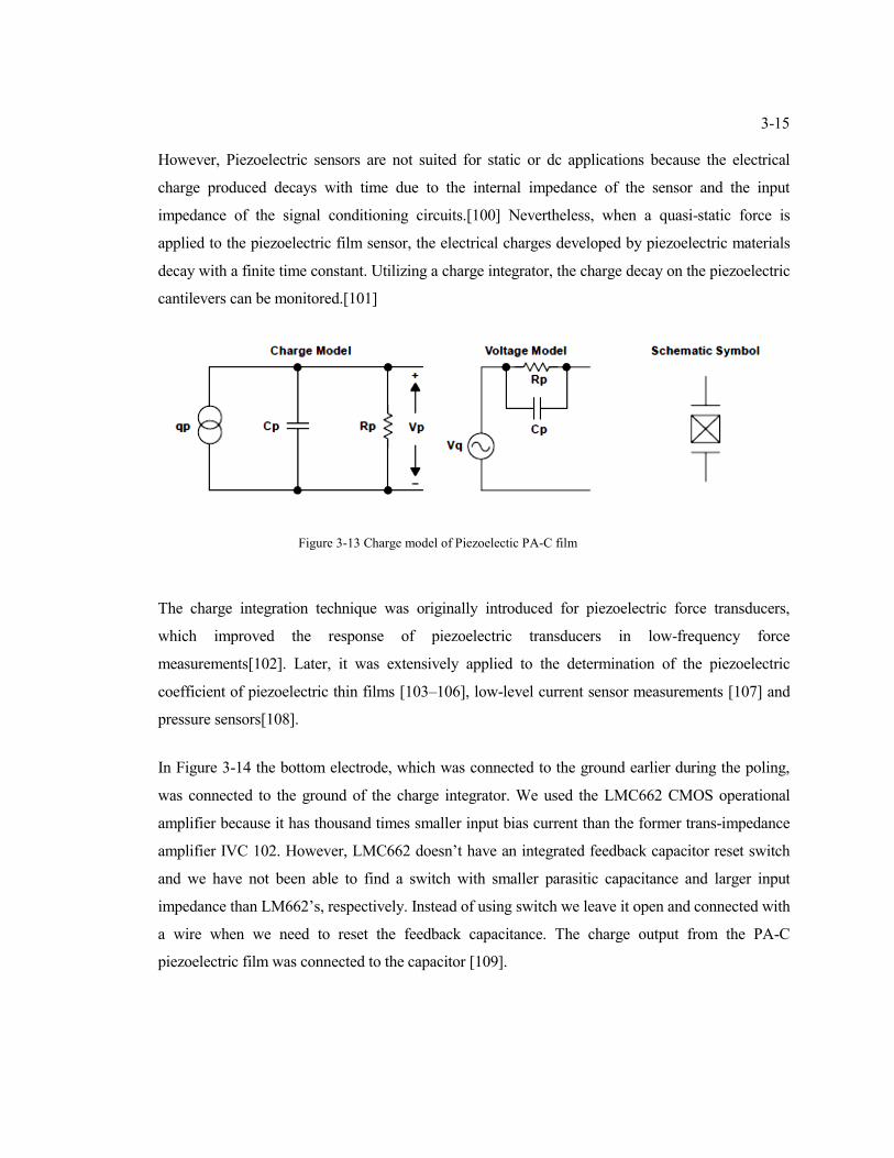
Figure 3-12 Picture of the pressuring chamber. ............................................................................... 3-14
Figure 3-13 Charge model of Piezoelectic PA-C film ..................................................................... 3-15
Figure 3-14 The charge integrator circuit ......................................................................................... 3-16
Page 13
xiii
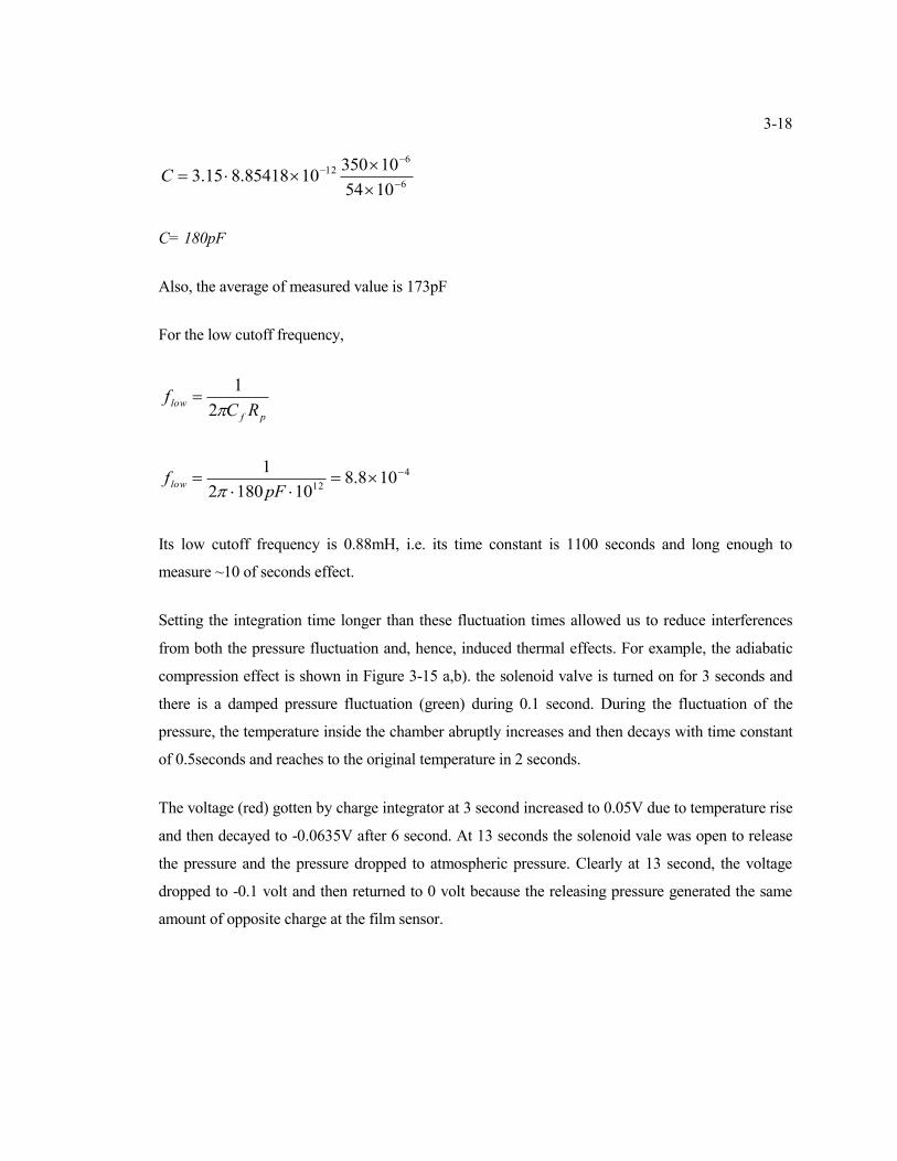
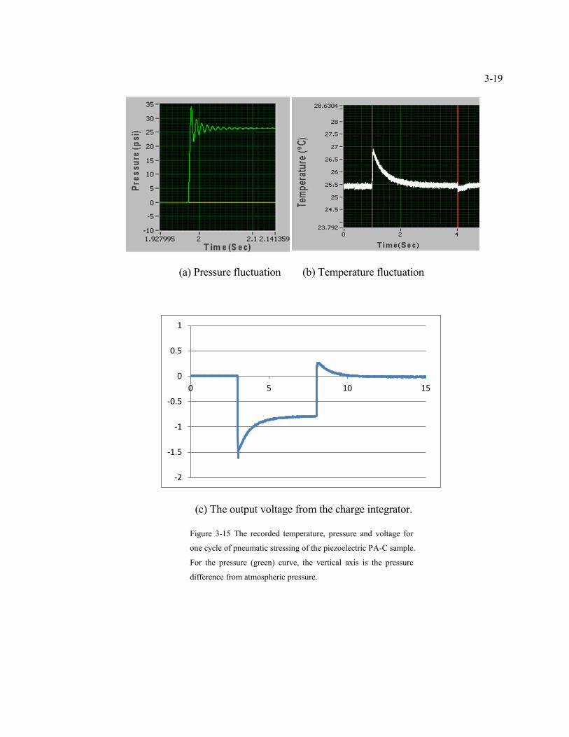
Figure 3-15 The recorded temperature, pressure and voltage for one cycle of pneumatic stressing of
the piezoelectric PA-C sample. For the pressure (green) curve, the vertical axis is the pressure
difference from atmospheric pressure. .............................................................................................. 3-19
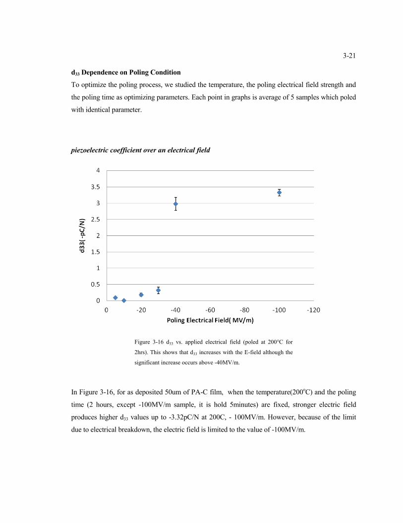
Figure 3-16 d33 vs. applied electrical field (poled at 200°C for 2hrs). This shows that d33 increases
with the E-field although the significant increase occurs above -40MV/m. ................................... 3-21
Figure 3-17 d33 vs. poling temperature (for 50um thick PA-C film, poled for 5 minutes with -
5.0kVm, i.e. -100MV/m). This shows that d33 peaks at 160°C. ....................................................... 3-22
Figure 3-18 Poling process is finished within 5 minutes. ................................................................ 3-23
Figure 3-19 Ageing effect on Piezoelectric PA-C film .................................................................... 3-24
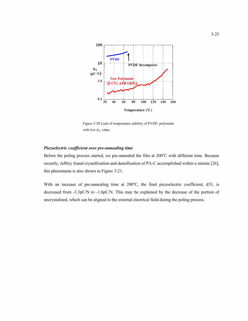
Figure 3-20 Lack of temperature stability of PVDF; polyimide with low d31 value ....................... 3-25
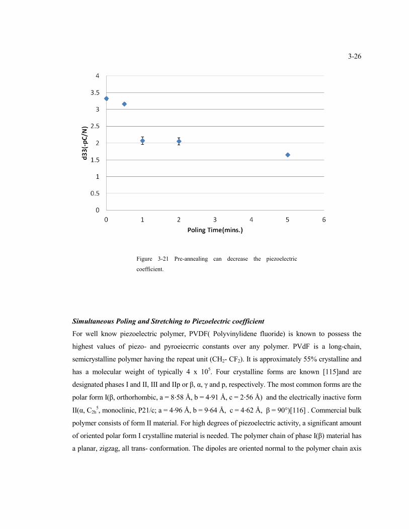
Figure 3-21 Pre-annealing can decrease the piezoelectric coefficient. ............................................ 3-26
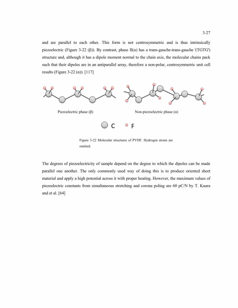
Figure 3-22 Molecular structures of PVDF. Hydrogen atoms are omitted. .................................... 3-27
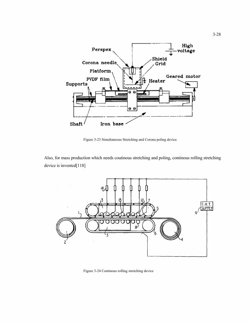
Figure 3-23 Simultaneous Stretching and Corona poling device. ................................................... 3-28
Figure 3-24 Continous rolling stretching device .............................................................................. 3-28
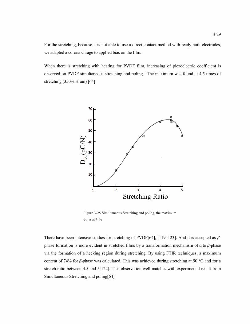
Figure 3-25 Simultaneous Stretching and poling, the maximum d31 is at 4.5X ............................... 3-29
Figure 3-26 Schematics of stretching setup. ..................................................................................... 3-30
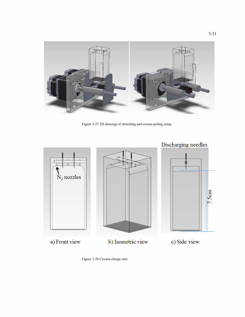
Figure 3-27 3D drawing of stretching and corona poling setup....................................................... 3-31
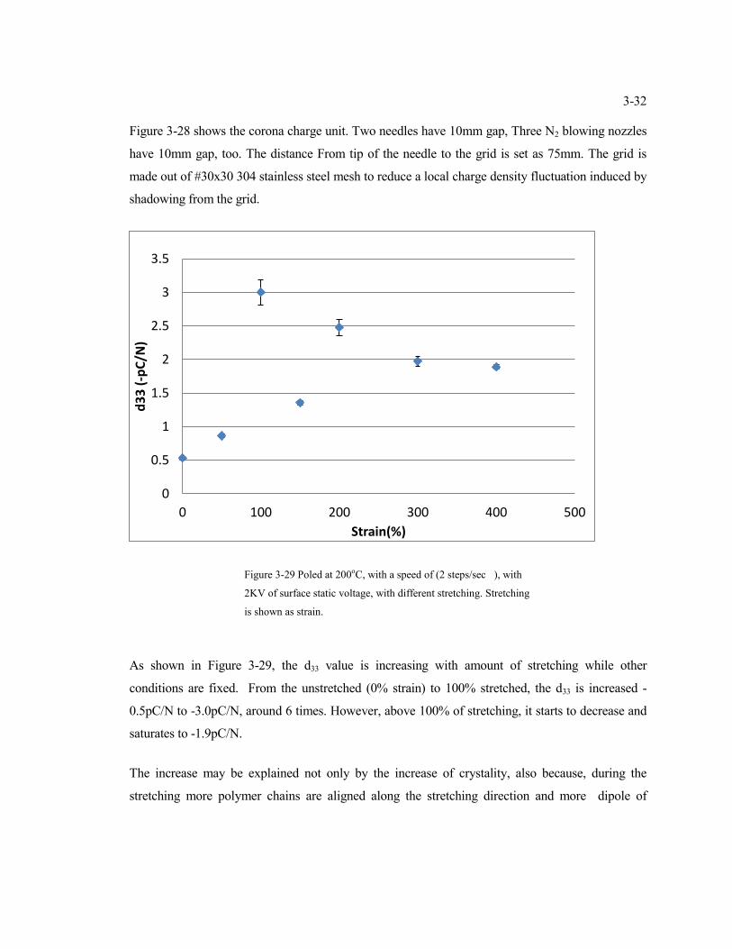
Figure 3-28 Corona charge unit. ....................................................................................................... 3-31
Figure 3-29 Poled at 200oC, with a speed of (2 steps/sec ), with 2KV of surface static voltage, with
different stretching. Stretching is shown as strain. ........................................................................... 3-32
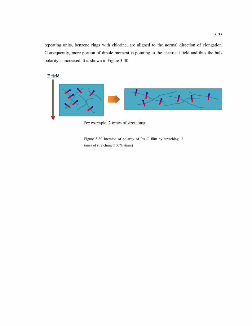
Figure 3-30 Increase of polarity of PA-C film by stretching. 2 times of stretching (100% strain) 3-33
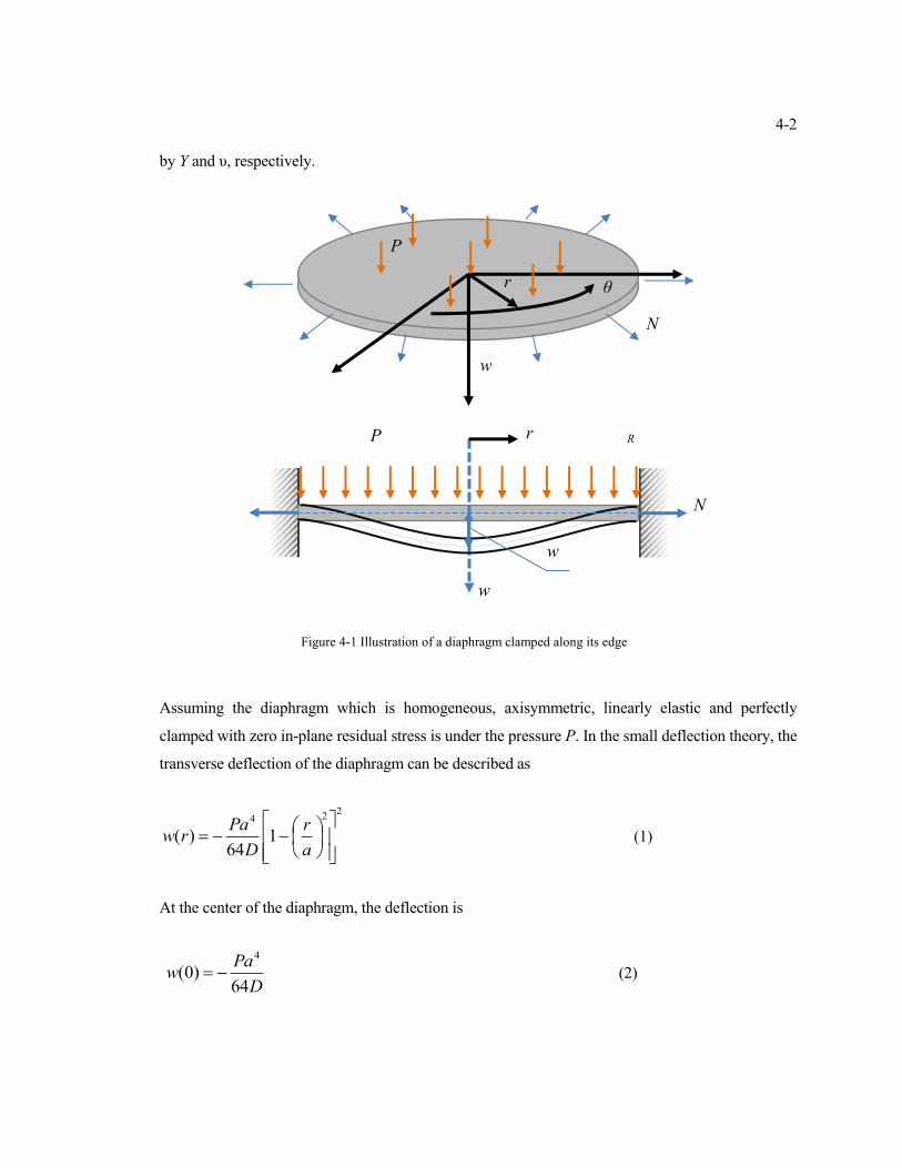
Figure 4-1 Illustration of a diaphragm clamped along its edge.......................................................... 4-2
Figure 4-2 α2*a over tension parameter k ........................................................................................... 4-7
Figure 4-3 Resonance frequency dependency over different radiuses (30um thick PA-C). ............. 4-9
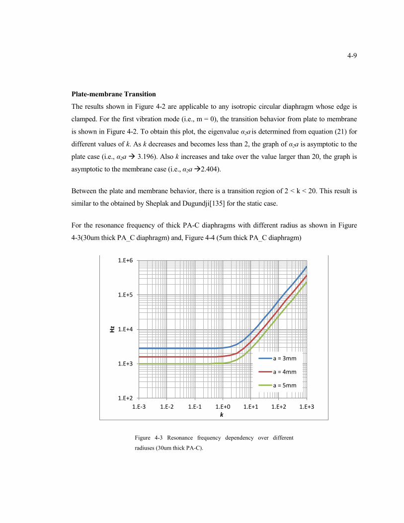
Figure 4-4 Resonance frequency dependency over different radiuses (5um thick PA-C). ............. 4-10
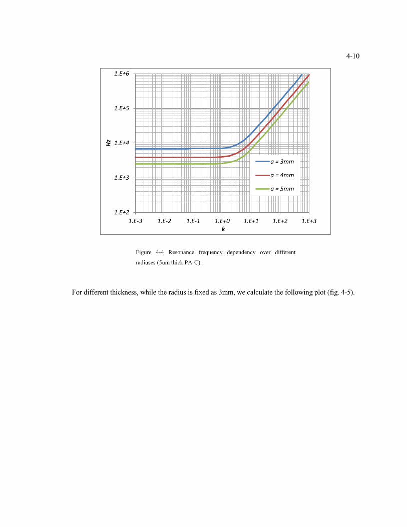
Figure 4-5 Resonance frequency dependency over different thickness (3mm in radius). .............. 4-11
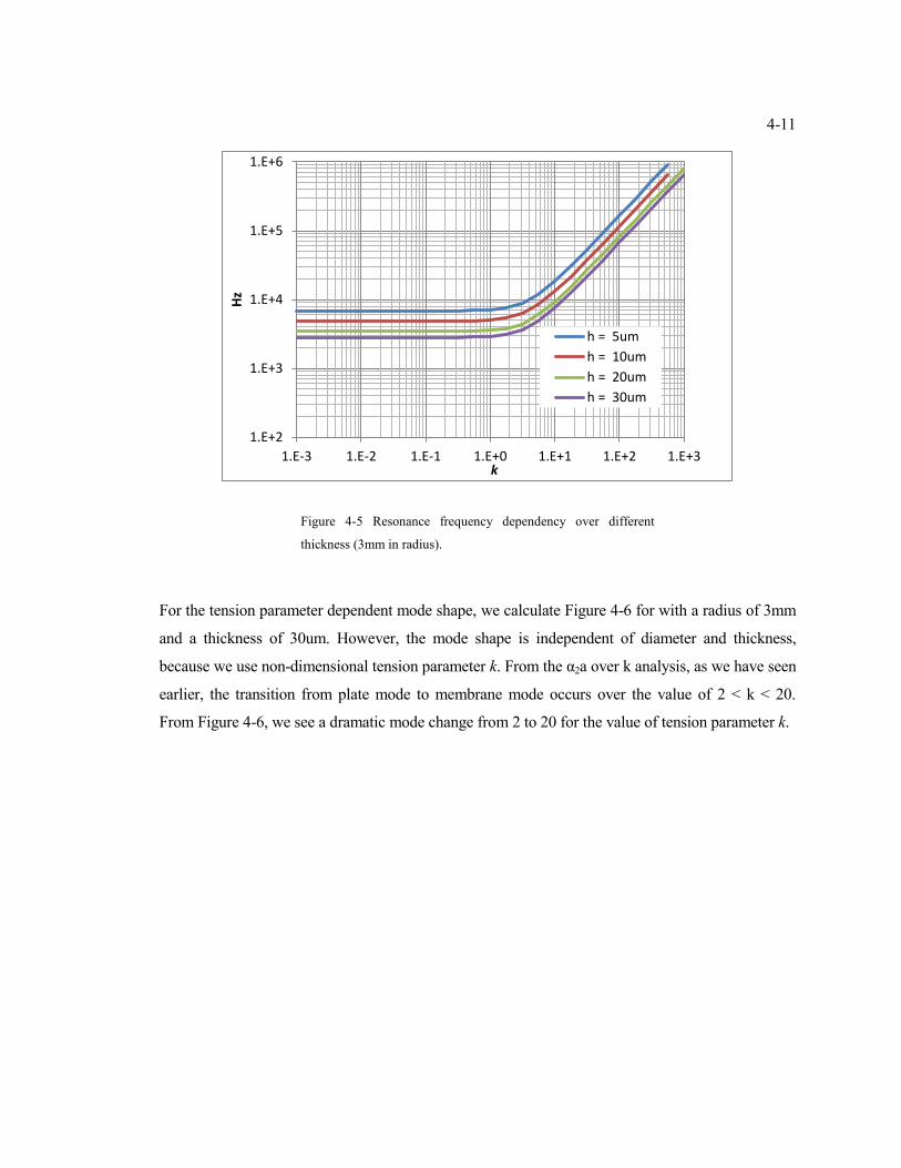
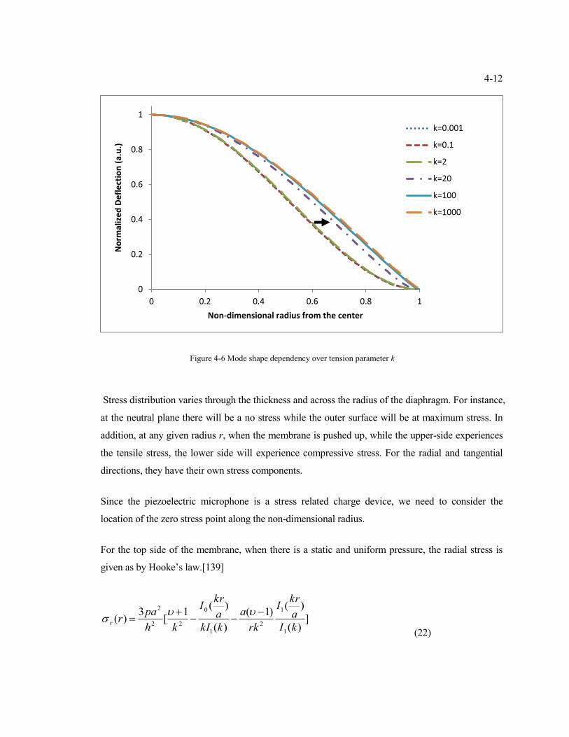
Figure 4-6 Mode shape dependency over tension parameter k ........................................................ 4-12
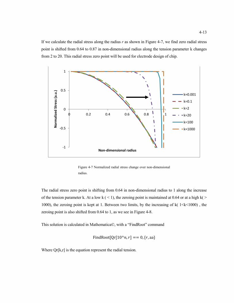
Figure 4-7 Normalized radial stress change over non-dimensional radius. ..................................... 4-13
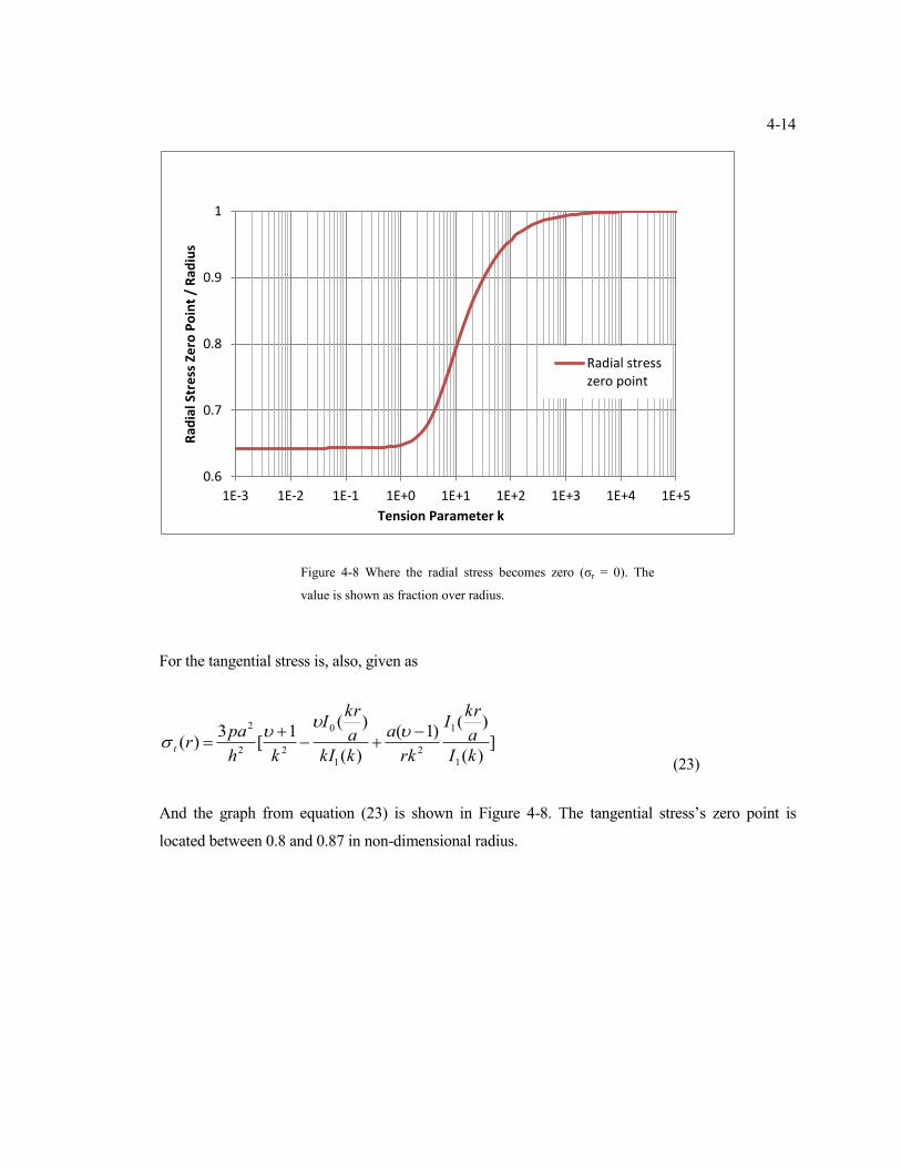
Figure 4-8 Where the radial stress becomes zero (σr = 0). The value is shown as fraction over radius.
............................................................................................................................................................ 4-14
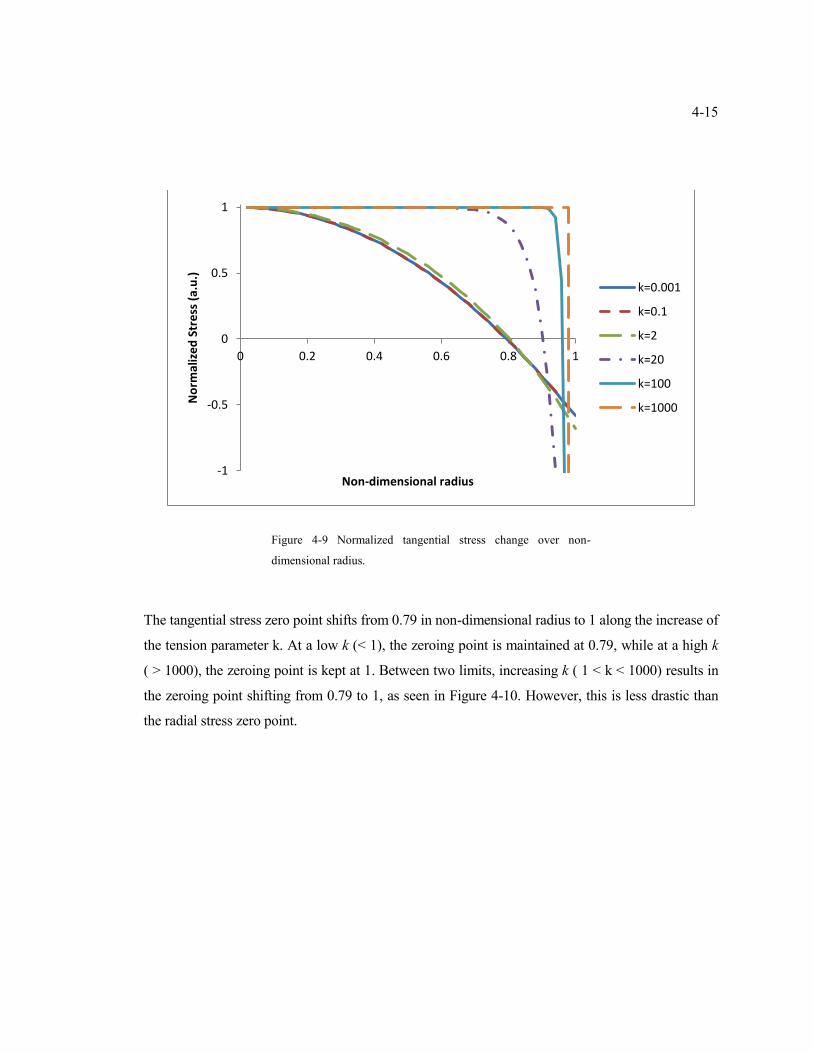
Figure 4-9 Normalized tangential stress change over non-dimensional radius. .............................. 4-15
Page 14
xiv
Figure 4-10 Where the Tangential stress becomes zero (σt = 0). The value is shown as fraction over
radius. ................................................................................................................................................. 4-16
Figure 4-11 Static pressure inducing the deflection of the diaphragm, after the process................ 4-18
Figure 4-12 Static pressure inducing the deflection of the diaphragm, after a annealing at 160oC, 1hr
............................................................................................................................................................ 4-18
Figure 4-13 Static pressure inducing the deflection of the diaphragm, after a annealing at 200oC, 5m
............................................................................................................................................................ 4-19
Figure 4-14: Experimental setup of the blister test: (a) the cross-section view of the test jig, and (b)
schematic diagram of the testing setup ............................................................................................. 4-21
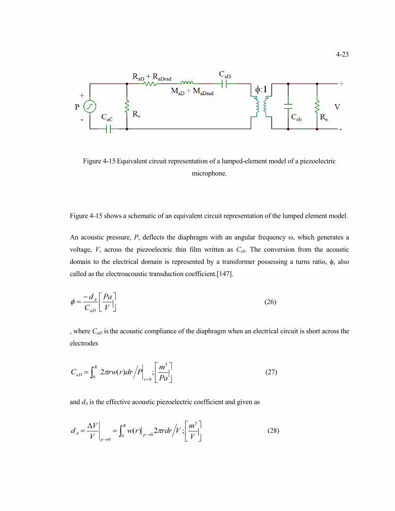
Figure 4-15 Equivalent circuit representation of a lumped-element model of a piezoelectric
microphone. ....................................................................................................................................... 4-23
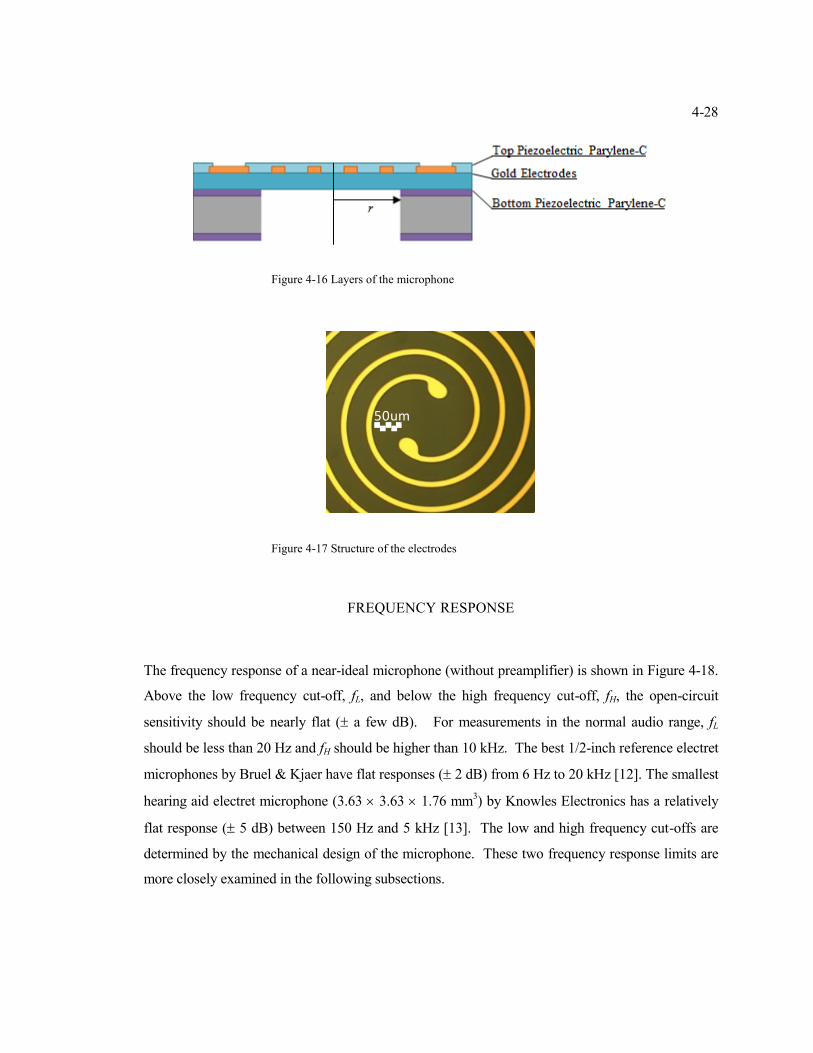
Figure 4-16 Layers of the microphone ............................................................................................. 4-28
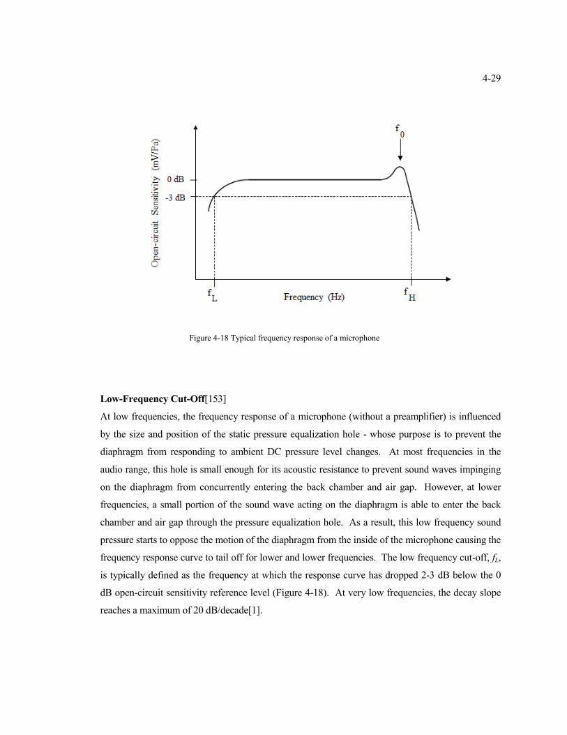
Figure 4-17 Structure of the electrodes ............................................................................................. 4-28
Figure 4-18 Typical frequency response of a microphone ............................................................... 4-29
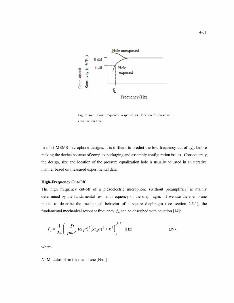
Figure 4-19 Pressure equalization hole positions. (a) Hole exposed. (b) Hole unexposed. ............ 4-30
Figure 4-20 Low frequency response vs. location of pressure equalization hole. ........................... 4-31
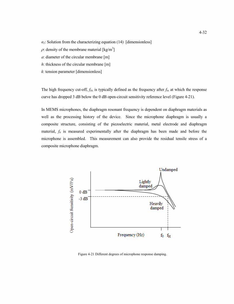
Figure 4-21 Different degrees of microphone response damping. ................................................... 4-32
Figure 5-1 Overall processes ............................................................................................................... 5-4
Figure 5-2 Wet thermal oxidation data ............................................................................................... 5-5
Figure 5-3 DRIE process ..................................................................................................................... 5-7
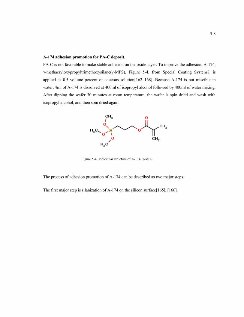
Figure 5-4. Molecular structure of A-174, γ-MPS ............................................................................. 5-8
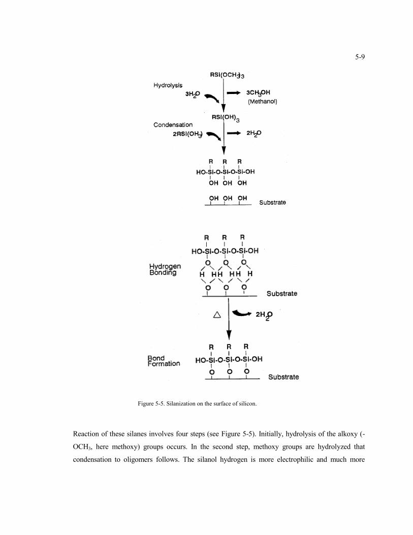
Figure 5-5. Silanization on the surface of silicon. .............................................................................. 5-9
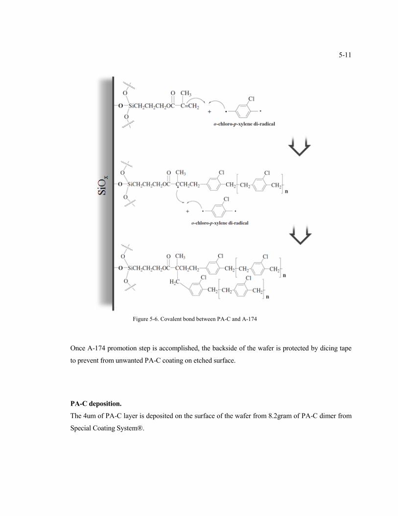
Figure 5-6. Covalent bond between PA-C and A-174 ..................................................................... 5-11
Figure 5-7. The deposition process of PA-C .................................................................................... 5-12
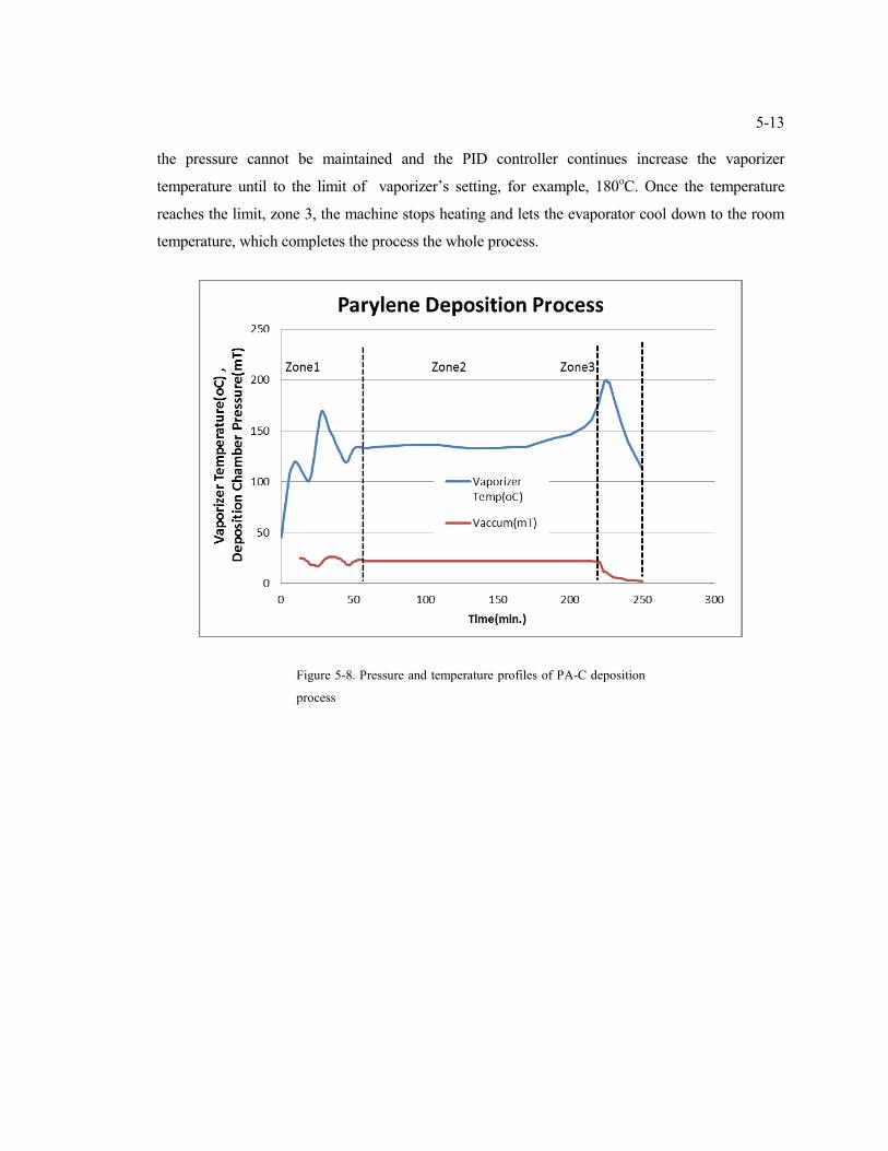
Figure 5-8. Pressure and temperature profiles of PA-C deposition process .................................... 5-13
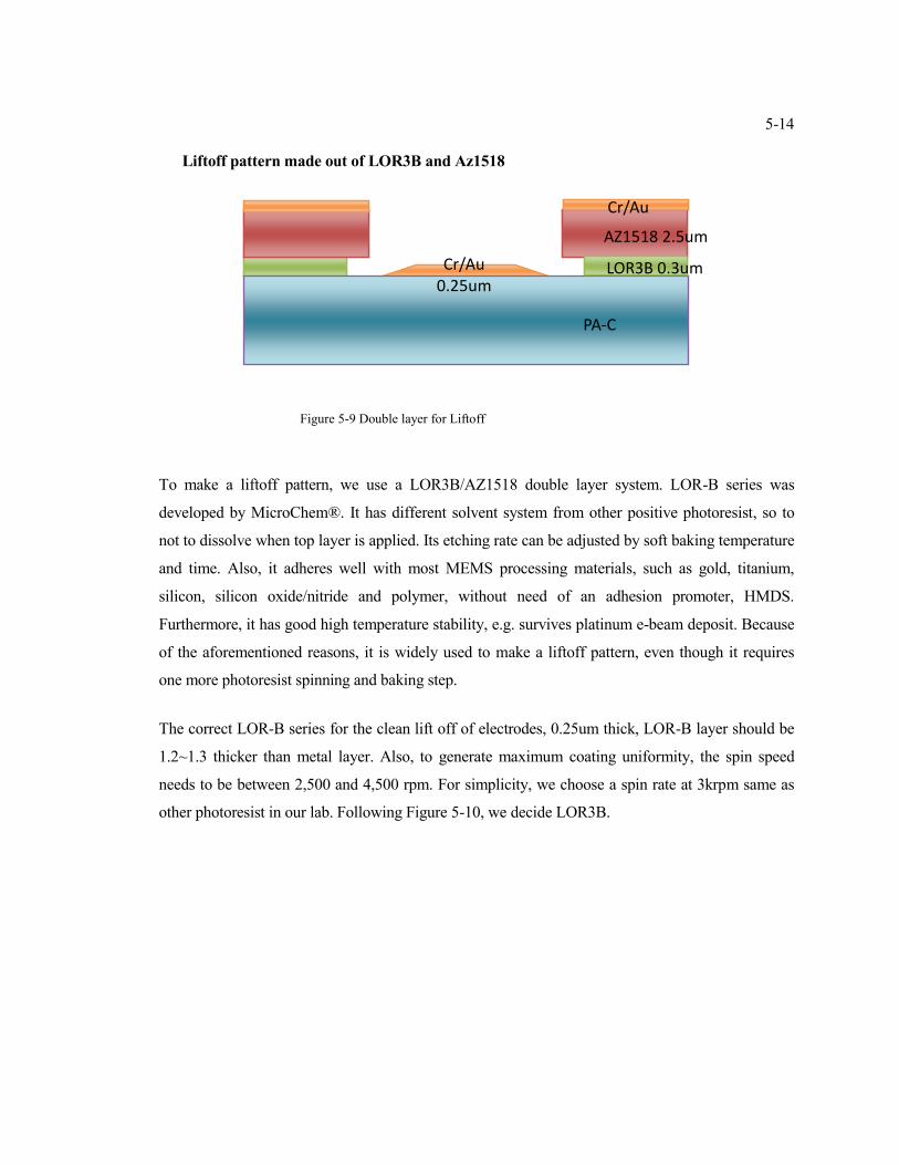
Figure 5-9 Double layer for Liftoff ................................................................................................... 5-14
Figure 5-10. Spin speed vs thickness for LOR B series resists. ....................................................... 5-15
Figure 5-11 Liftoff pattern delamination from poor LOR3B adhesion, baked at 140oC, 5min. .... 5-16
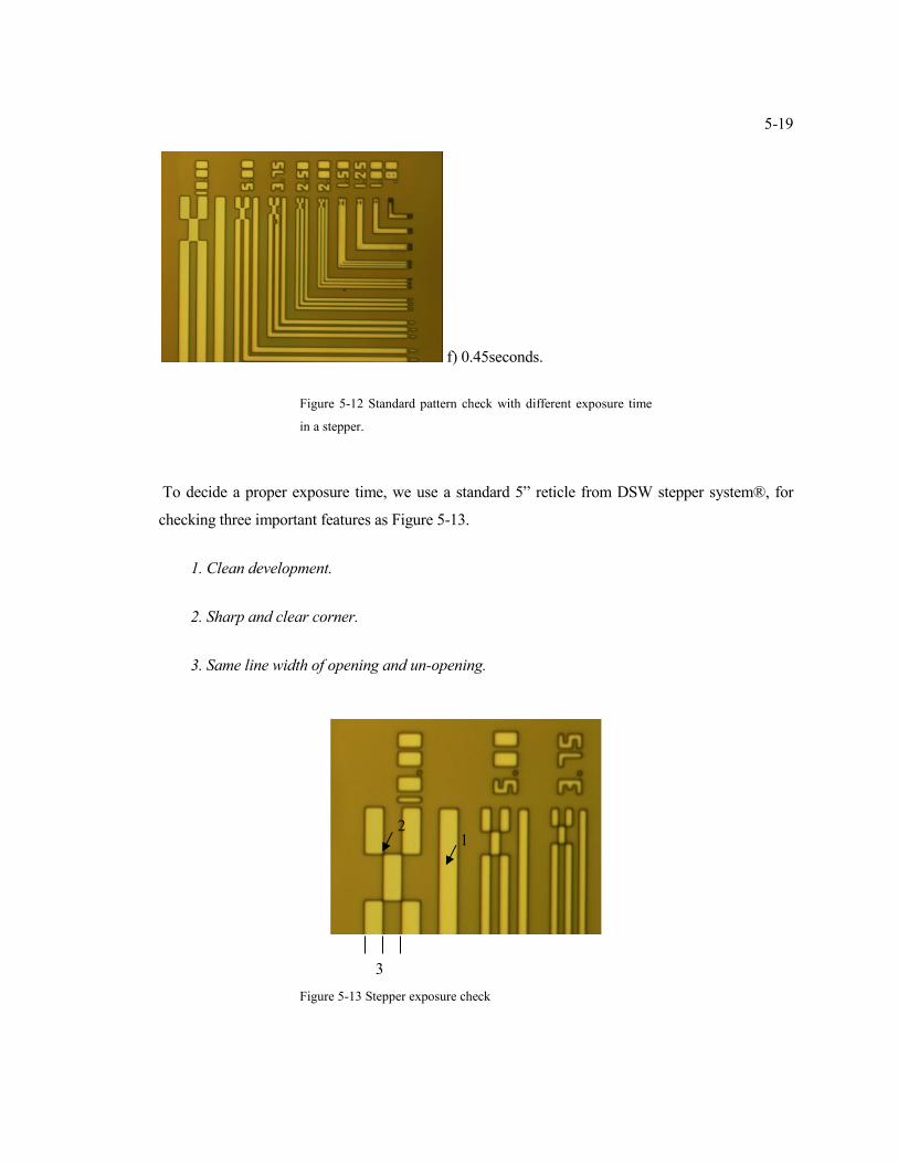
Figure 5-12 Standard pattern check with different exposure time in a stepper. .............................. 5-19
Figure 5-13 Stepper exposure check ................................................................................................. 5-19
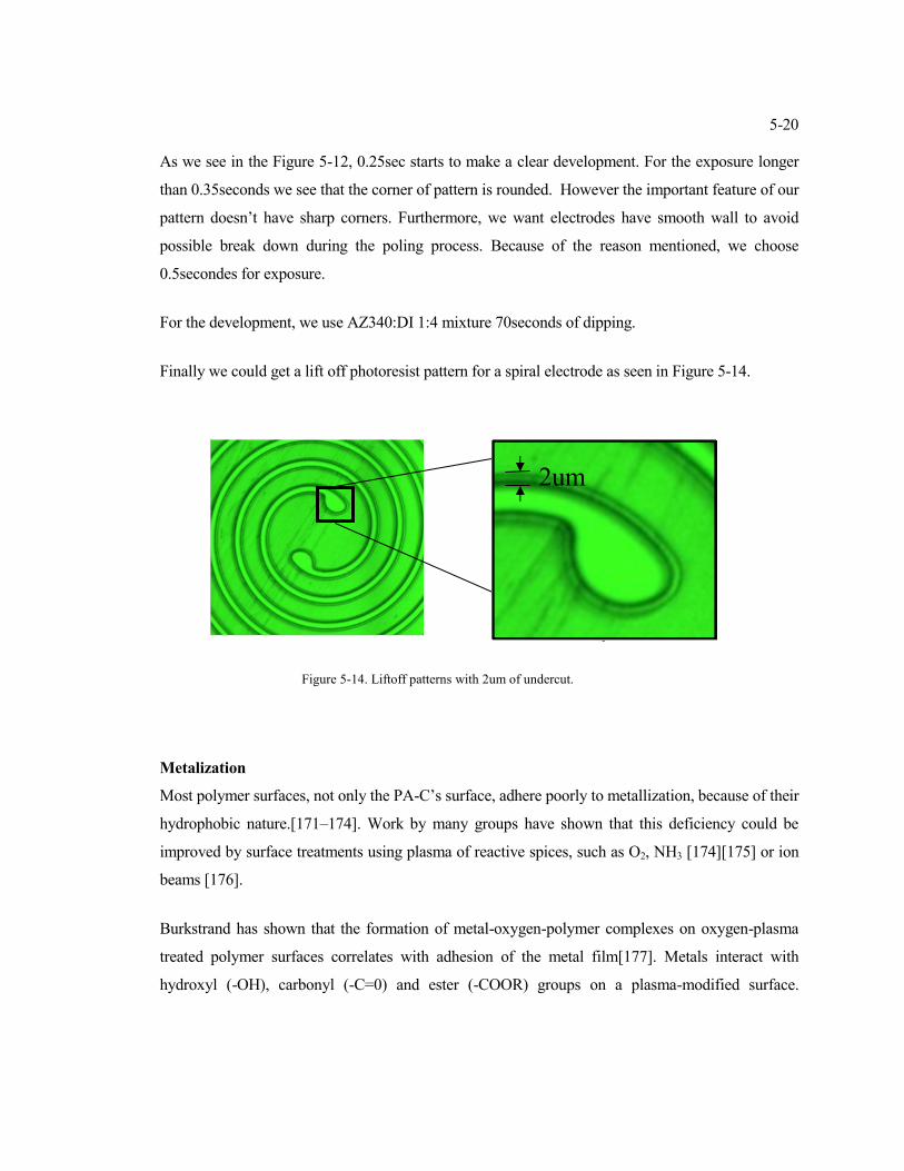
Figure 5-14. Liftoff patterns with 2um of undercut.......................................................................... 5-20
Page 15
xv
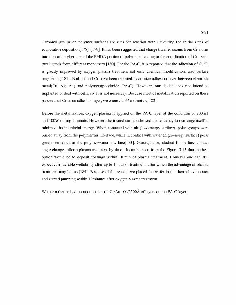
Figure 5-15. Variation of contact angle with time on polycarbonate substrate after plasma treatment.
............................................................................................................................................................ 5-22
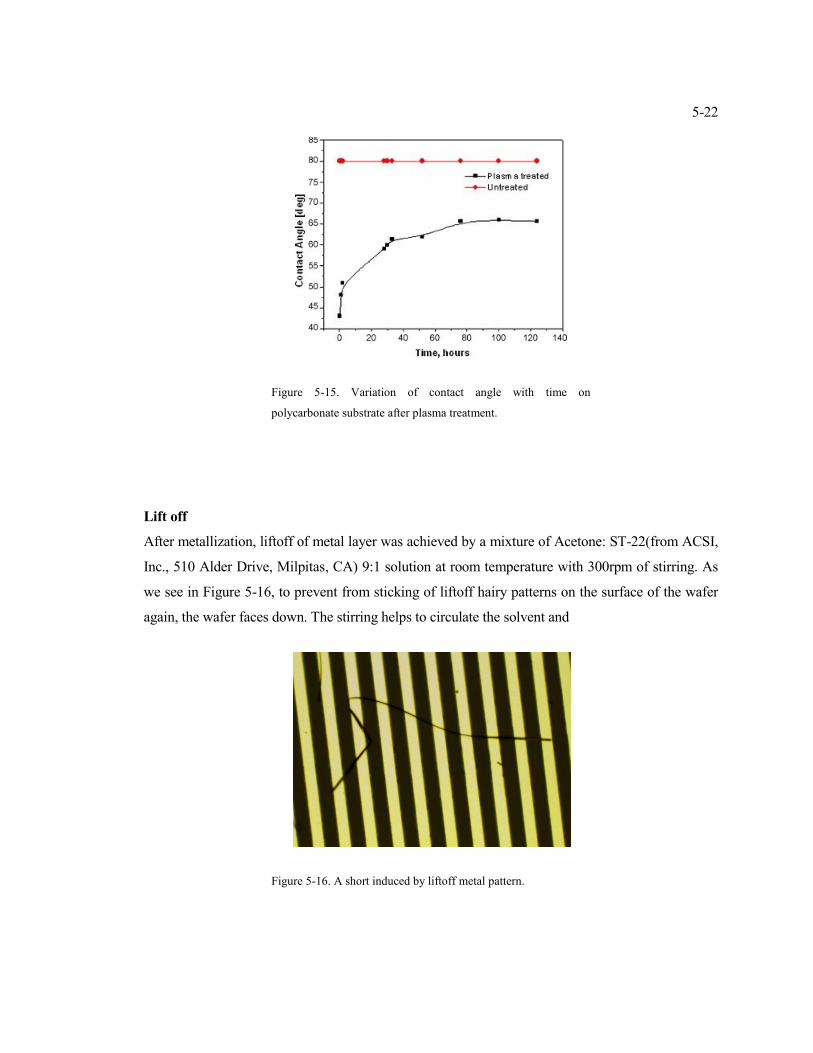
Figure 5-16. A short induced by liftoff metal pattern. ..................................................................... 5-22
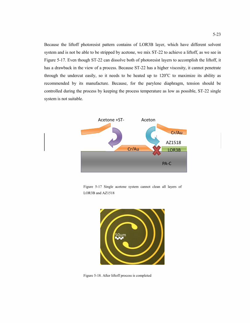
Figure 5-17 Single acetone system cannot clean all layers of LOR3B and AZ1518 ...................... 5-23
Figure 5-18. After liftoff process is completed ................................................................................ 5-23
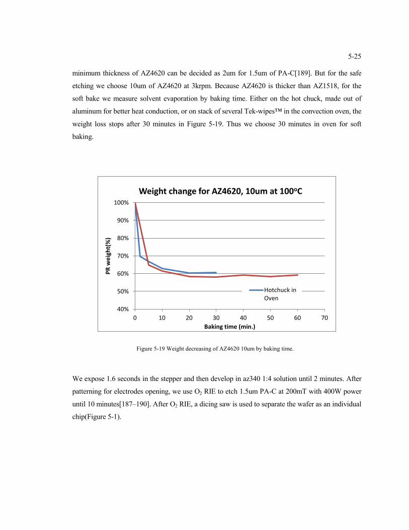
Figure 5-19 Weight decreasing of AZ4620 10um by baking time. ................................................. 5-25
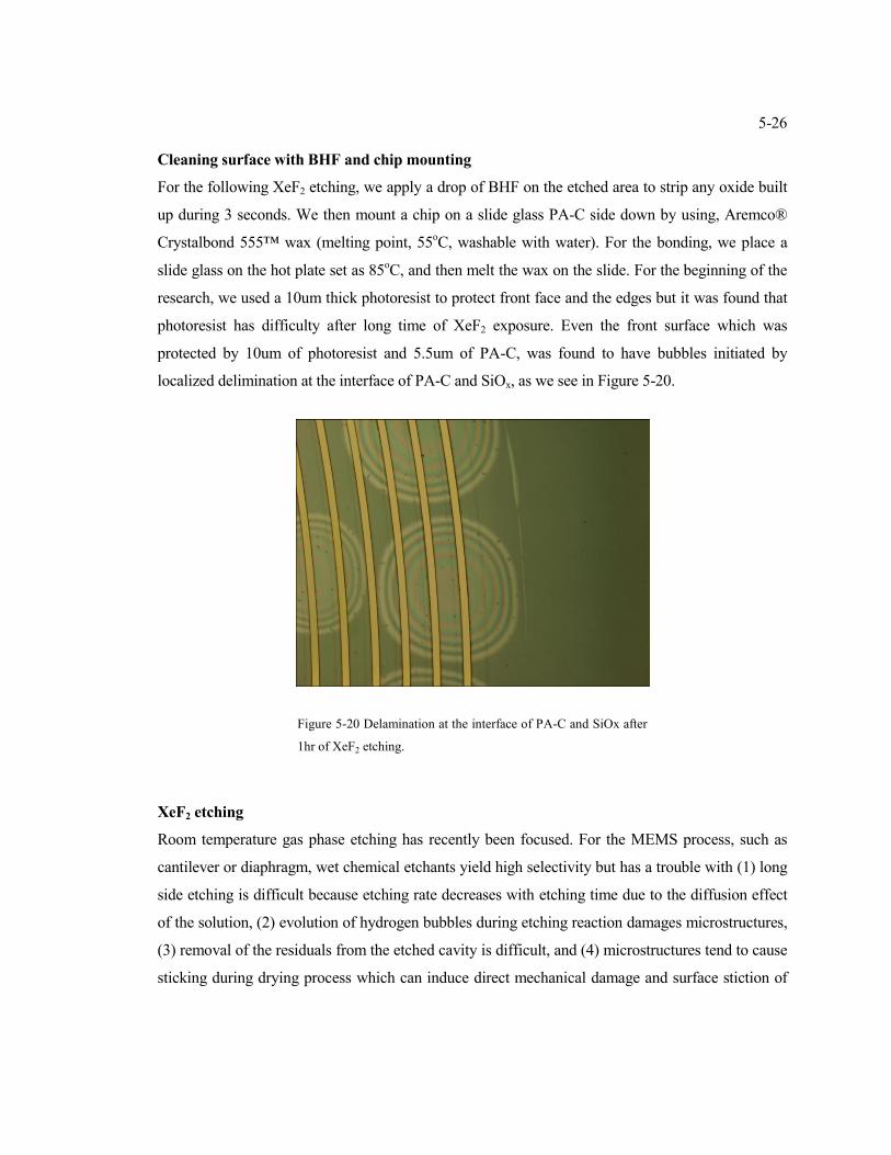
Figure 5-20 Delamination at the interface of PA-C and SiOx after 1hr of XeF2 etching. .............. 5-26
Figure 5-25 Ball model of XeF2 ........................................................................................................ 5-28
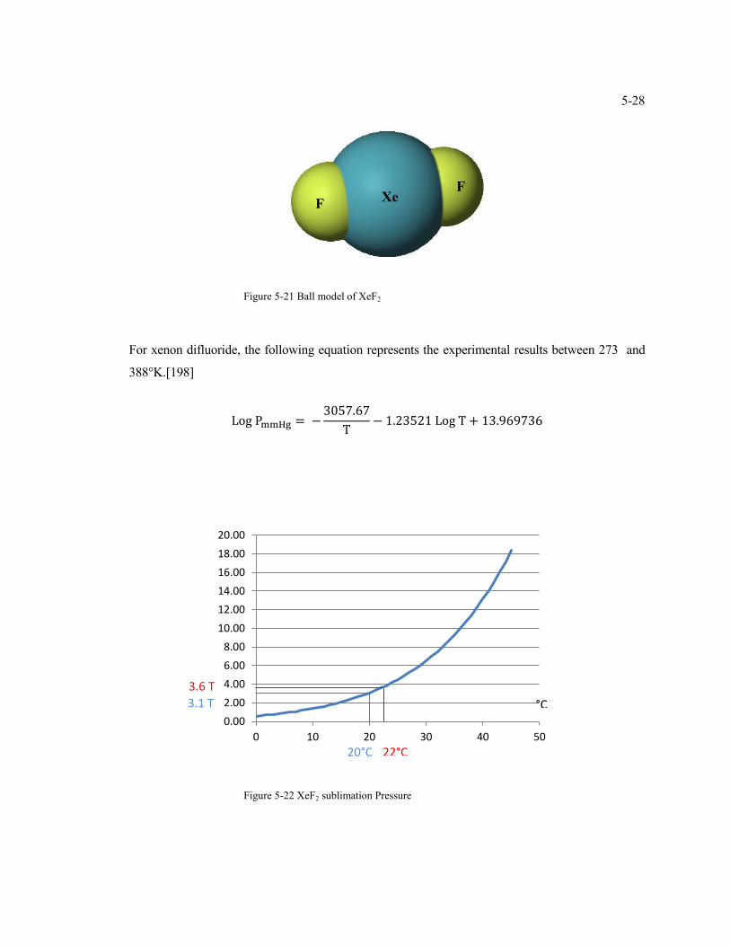
Figure 5-26 XeF2 sublimation Pressure ............................................................................................ 5-28
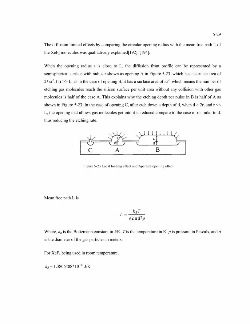
Figure 5-27 Local loading effect and Aperture opening effect ........................................................ 5-29
Figure 5-28 Schematics of XeF2 etching system .............................................................................. 5-31
Figure 5-29 A setup for poling process. ........................................................................................... 5-32
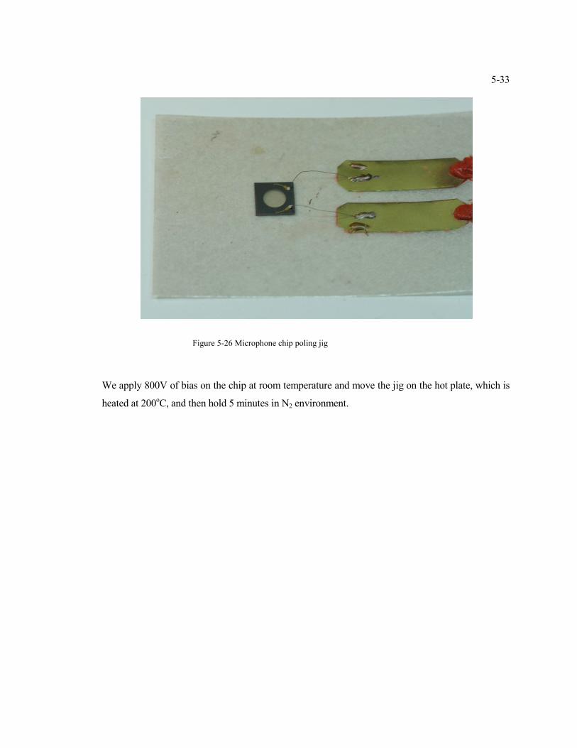
Figure 5-30 Microphone chip poling jig ........................................................................................... 5-33
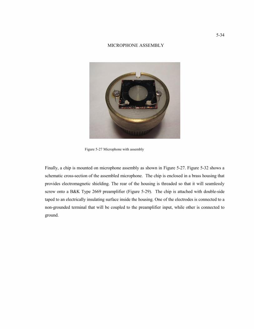
Figure 5-31 Microphone with assembly ........................................................................................... 5-34
Figure 5-32 Schematic of microphone assembly ............................................................................. 5-35
Figure 5-33 a) Microphone housing, b) with preamplifier............................................................... 5-35
Figure 5-34 Structure of a DVD/CD pick-up head. ......................................................................... 5-37
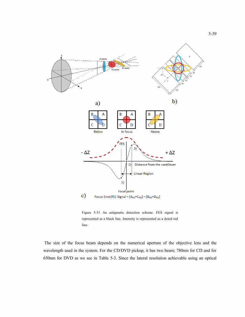
Figure 5-35 An astigmatic detection scheme. FES signal is represented as a black line. Intensity is
represented as a doted red line. ......................................................................................................... 5-39
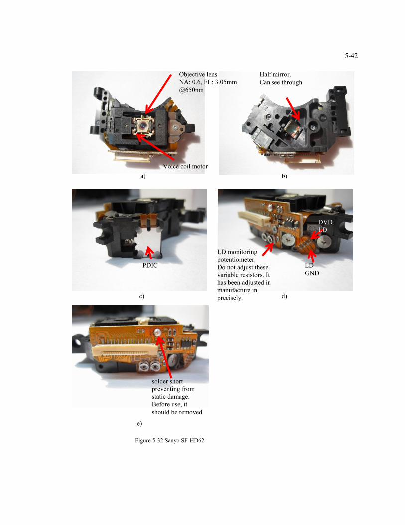
Figure 5-36 Sanyo SF-HD62 ............................................................................................................ 5-42
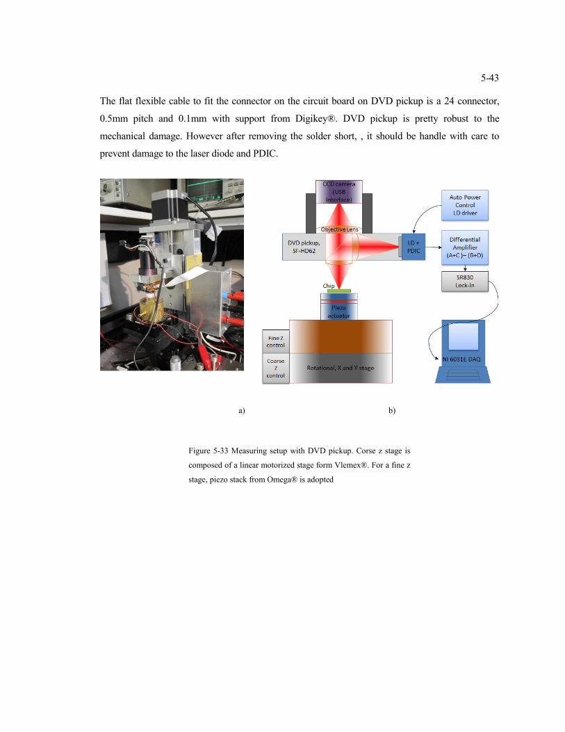
Figure 5-37 Measuring setup with DVD pickup. Corse z stage is composed of a linear motorized
stage form Vlemex® . For a fine z stage, piezo stack from Omega® is adopted ............................ 5-43
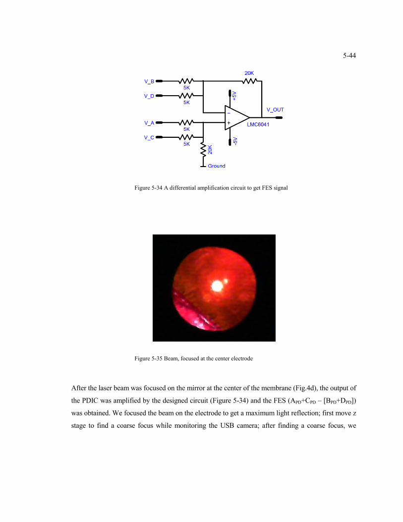
Figure 5-38 A differential amplification circuit to get FES signal .................................................. 5-44
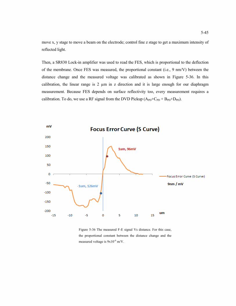
Figure 5-39 Beam, focused at the center electrode .......................................................................... 5-44
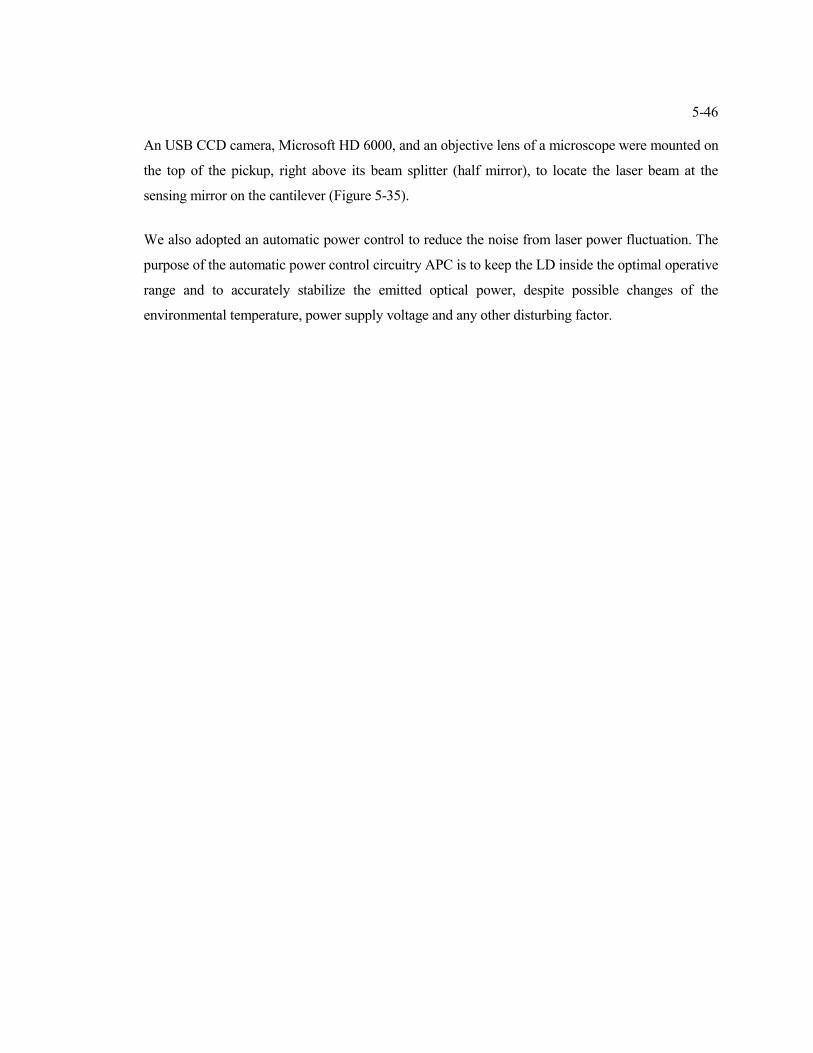
Figure 5-40 The measured F-E signal Vs distance. For this case, the proportional constant between
the distance change and the measured voltage is 9x10⁻⁶ m/V. ......................................................... 5-45
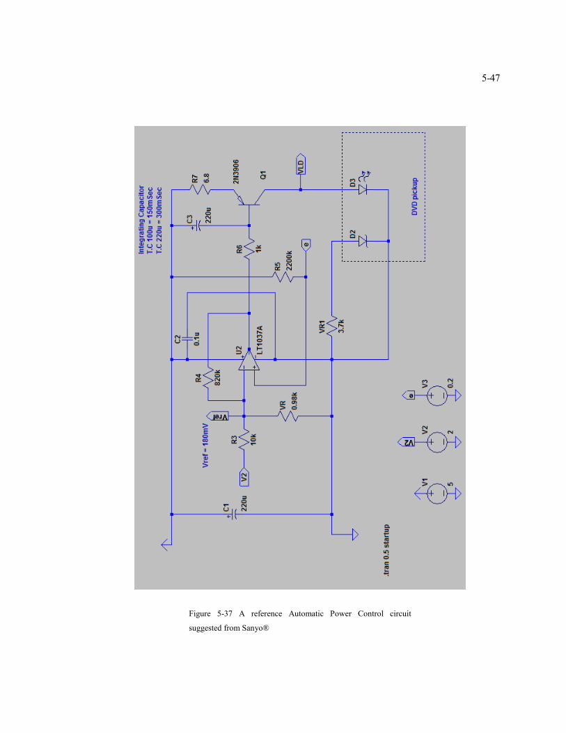
Figure 5-41 A reference Automatic Power Control circuit suggested from Sanyo® ..................... 5-47
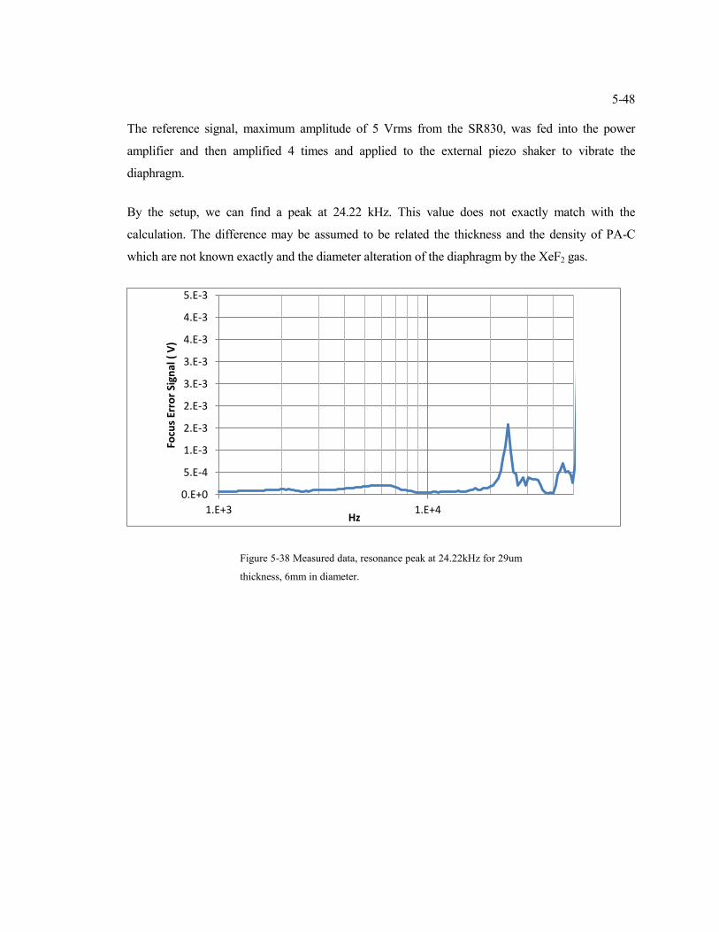
Figure 5-42 Measured data, resonance peak at 24.22kHz for 29um thickness, 6mm in diameter. 5-48
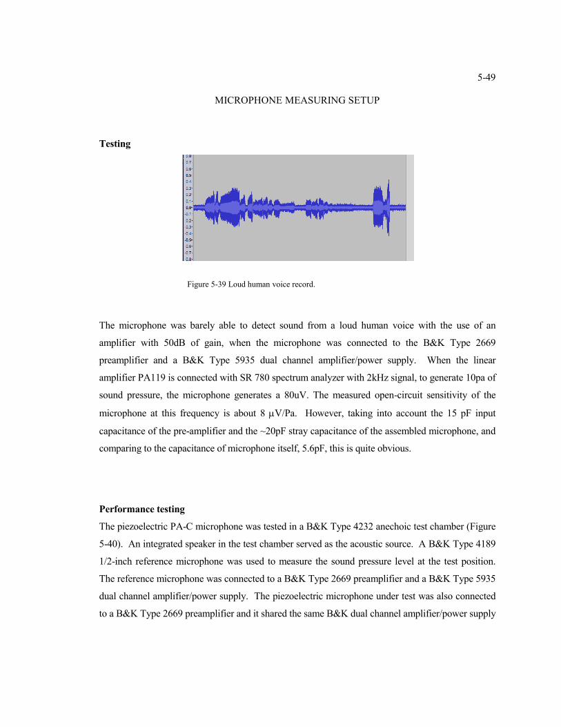
Figure 5-43 Loud human voice record. ............................................................................................ 5-49
Figure 5-44 Measuring setup. ........................................................................................................... 5-50
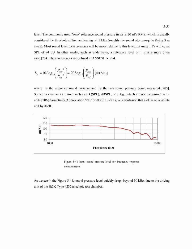
Figure 5-45 Input sound pressure level for frequency response measurements .............................. 5-51
Page 16
xvi
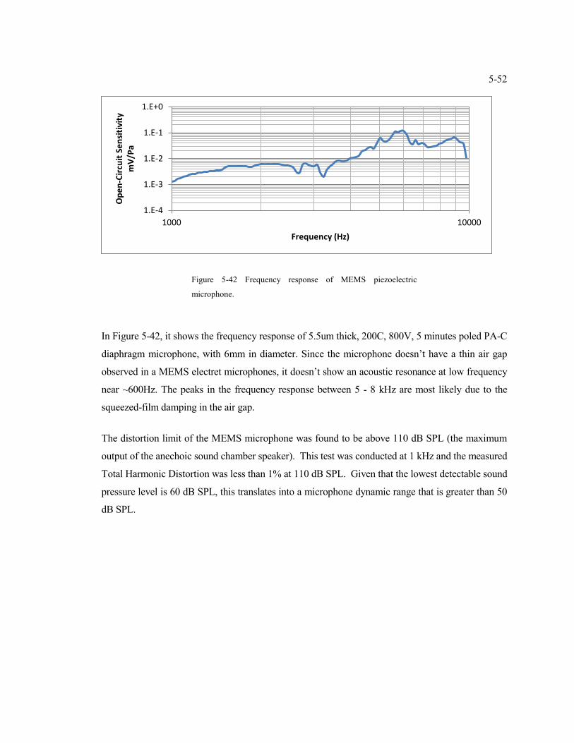
Figure 5-46 Frequency response of MEMS piezoelectric microphone. .......................................... 5-52
Page 17
xvii
LIST OF TABLES
Number Page
Table 3-1 Properties of Parylene N, C and D [1]. .............................................................................. 3-3
Table 4-1 Measured residual tension after process and after poling process. * The maximum
temperature which the device experienced during the fabrication is 150oC, 5 minutes. ................. 4-19
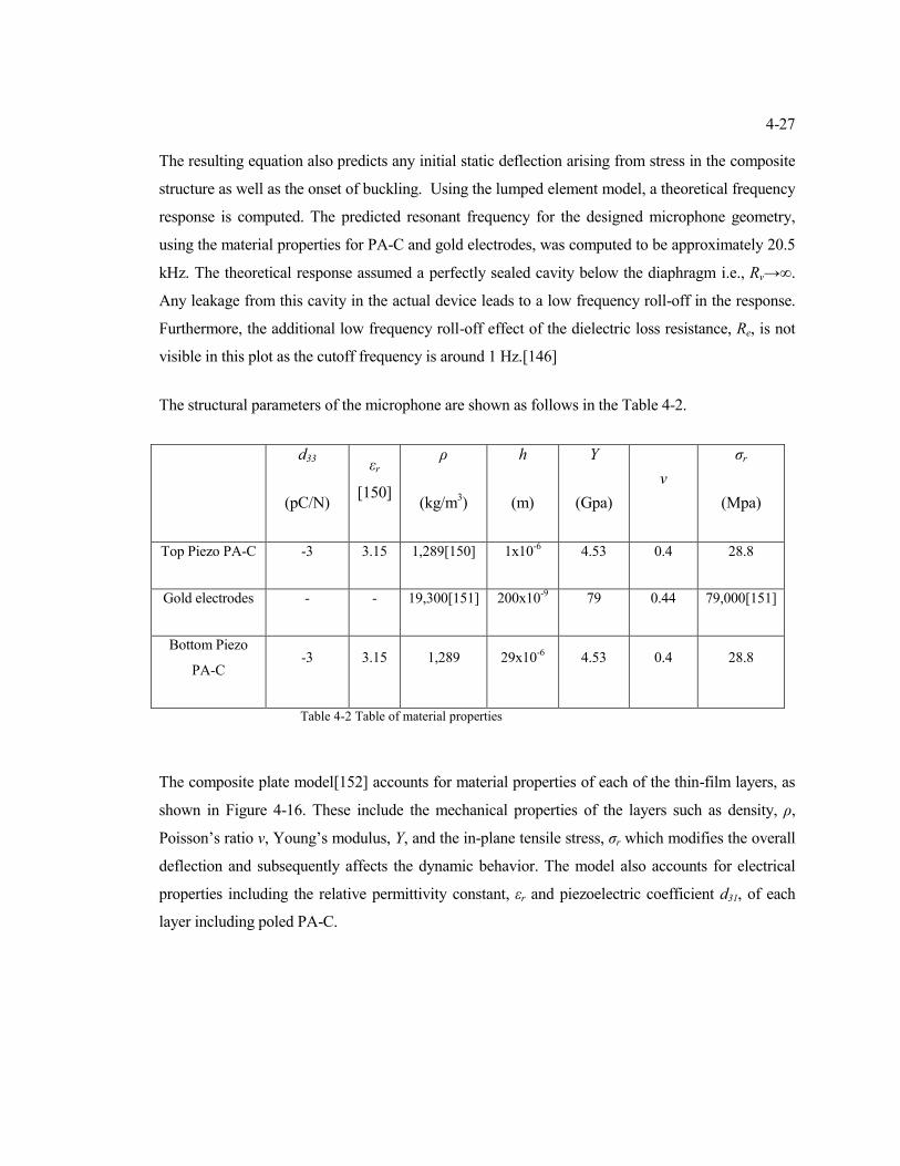
Table 4-2 Table of material properties .............................................................................................. 4-27
Table 5-1 LOR3B baking test (baked on a hot plate) ....................................................................... 5-16
Table 5-4 XeF2 Etching depends on Materials ................................................................................. 5-27
Table 5-5 Specifications of the DVD optical pickup head white paper. ......................................... 5-36
Table 5-6 Pin connection of Sanyo SF-HD62, A,B,C,D for DVD mode, a,b,c,d for CD mode are
used to generate FES signal; Pin 8, RF represents intensity of light used to figure out the maximum
reflecting point. .................................................................................................................................. 5-41
Page 18
1-1
C h a p t e r 1
INTRODUCTION
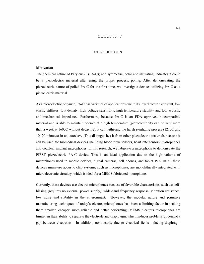
Motivation
The chemical nature of Parylene-C (PA-C); non symmetric, polar and insulating, indicates it could
be a piezoelectric material after using the proper process, poling. After demonstrating the
piezoelectric nature of polled PA-C for the first time, we investigate devices utilizing PA-C as a
piezoelectric material.
As a piezoelectric polymer, PA-C has varieties of applications due to its low dielectric constant, low
elastic stiffness, low density, high voltage sensitivity, high temperature stability and low acoustic
and mechanical impedance. Furthermore, because PA-C is an FDA approved biocompatible
material and is able to maintain operate at a high temperature (piezoelectricity can be kept more
than a week at 160oC without decaying), it can withstand the harsh sterilizing process (121oC and
10~20 minutes) in an autoclave. This distinguishes it from other piezoelectric materials because it
can be used for biomedical devices including blood flow sensors, heart rate sensors, hydrophones
and cochlear implant microphones. In this research, we fabricate a microphone to demonstrate the
FIRST piezoelectric PA-C device. This is an ideal application due to the high volume of
microphones used in mobile devices, digital cameras, cell phones, and tablet PCs. In all these
devices miniature acoustic chip systems, such as microphones, are monolithically integrated with
microelectronic circuitry, which is ideal for a MEMS fabricated microphone.
Currently, these devices use electret microphones because of favorable characteristics such as: self-
biasing (requires no external power supply), wide-band frequency response, vibration resistance,
low noise and stability in the environment. However, the modular nature and primitive
manufacturing techniques of today’s electret microphones has been a limiting factor in making
them smaller, cheaper, more reliable and better performing. MEMS electrets microphones are
limited in their ability to separate the electrode and diaphragm, which induces problems of control a
gap between electrodes. In addition, nonlinearity due to electrical fields inducing diaphragm
Page 19
1-2
stiffness, and sensitivity to environmental change, dust, moisture and shock also limit performance.
Furthermore, wafer bonding or removing of sacrificial layer is necessary and this becomes a
limiting factor to the low cost and productivity.
Compared with the electrets microphone, the piezoelectric microphone has only one diaphragm and
it brings several advantages including robustness to shock and dust, and producibility. Also, by the
nature of the piezoelectric effect, it has a wide bandwidth, high output impedance, large dynamic
range, and is robust from electromagnetic interference, even though it has a lower sensitivity than
the electret microphone.
Combined with MEMS technology, the piezoelectric microphone has additional advantages
including
high degree of miniaturization with no or minimal loss in performance
repeatable and precise dimensional control
high volume manufacturing with a high degree of reproducibility
ability to array multiple microphones on the same substrate
ability to integrate with on-chip microelectronics
freedom to choose from a wide range of materials and processing techniques.
Piezoelectric material
In 1820 Becquerel described and observed piezoelectric effect[1] although a systematic study
leading to modern understanding of these effects is credited to the Curies.[2] The two physicists
found that the surfaces of certain crystals became electrically charged when the crystal is
mechanically loaded.
Page 20
1-3
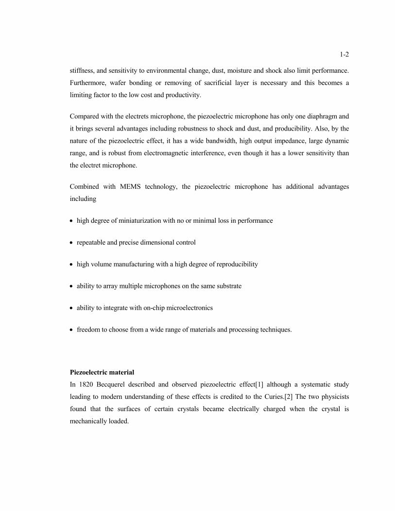
The Rochelle Salt transducer by Sawyer in 1931 is considered as the first practical invention of the
piezoelectric microphone.[3] The microphone uses a thin strip of piezoelectric material attached to a
diaphragm. The two sides of the crystal acquire opposite charges when the diaphragm deflects the
crystal. This bimorph idea has been widely used in low cost microphones since this invention.
However, due to water solubility, low melting temperature and fragile nature, the Rochelle salt
bimorph microphone has a poor environmental stability. It is quickly substituted with other
piezoelectric ceramic materials, such as Barium Titanate ceramics of Gray[4] and more recently by
PZT ceramics of Jaffe.[5]
Figure 1-1 Rochelle salt transducer, diaphragm type
Inorganic ceramic piezoelectric materials are characterized by mechanical hardness, high
piezoelectric coefficients, thermal and humidity stability. Organic piezoelectric materials have
lower piezoelectric coefficients than inorganic ceramic piezoelectric materials. However, they have
the advantage of flexibility, low weight, low acoustic and mechanical impedance, and are generally
non-toxic.[6] Despite its outstanding piezoelectric property, PZT is currently facing global
restrictions due to its lead toxicity.
The piezoelectric strain constant (d33) for the polymers is lower (PVDF(Poly Vinyl DiFluoro),
30pC/N) than that of the ceramic (PZT, 300pC/N). However, due to their low Young’s modulus,
piezoelectric polymers (PVDF, 240mV-m/N) have much higher piezoelectric stress constants (g33)
than ceramics (PZT, 11mV-m/N), which indicates that they can be better sensors than ceramics.
Page 21
1-4
Piezoelectric polymeric sensors and actuators offer the advantage of processing flexibility because
they are lightweight, tough, readily manufactured into large areas, and can be cut and formed into
complex shapes. Polymers also exhibit high strength and high impact resistance.[7] Other notable
features of polymers are low dielectric constant, low elastic stiffness, and low density, which result
in a high voltage sensitivity (excellent sensor characteristic), and low acoustic and mechanical
impedance (crucial for medical and underwater applications).
Thus, for example, PVDF is widely used as sensor material in applications such as, traffic signal
control loop sensor buried under the load, musical instrument pickups, sports scoring, impact
printers, bearing wear sensors, fan flow sensor and accelerometers.[8] Polymers also typically
possess a high dielectric breakdown and high operating field strength, which means that they can
withstand much higher driving fields than ceramics.
Also, polymers offer the ability to become a thin layer, to be patterned and to achieve electrodes on
the film surface, and consequently to be poled only selected regions. Based on these features,
piezoelectric polymers possess their own established area for technical applications and useful
device configurations. In MEMS field, curable polyimide is also used to build a touch sensor array,
air flow sensor and vibration sensor [9–13].
However, even though the overwhelming piezoelectric property of PVDF over other piezoelectric
polymers, it lacks temperature stability and is limited to less than 80 °C. For high temperature
applications, polyimide-based MEMS devices are used [9–15]. However, polyimide is hydophilic,
which induces lower stability in high humidity environments. In addition, these films are cured in
convection or diffusion ovens at high enough temperatures (350-400°C)[16] to assure adequate
mechanical and electrical properties. These high temperatures can change the electrical properties
of the devices. If the cure temperature of these films were lowered there could be a reduction in the
film (and wafer) stress as well as a lower thermal budget for the devices. However, curing
polyimide films below 250°C has does not provide the mechanical, chemical, and dielectric
properties required for the final device operation parameters or mechanical and dielectric
protection.[17]
Page 22
1-5
Parylene
Parylene development started in 1947, by Michael Szwarc but the reaction yield was only a few
percent, and a more efficient route was developed in the 1950s by William F. Gorham and was
commercialized in 1965 by the Union Carbide Corporation [18]. The Parylene film deposition
process did not require a solvent and resulted in chemically resistant films free from pinholes[19],
[20]. Since the coating process takes place at ambient temperature in a mild vacuum, and because of
Parylene’s conformal properties, it has a wide variety of applications. Various types of Parylene
films have been extensively studied for numerous applications due to its mechanical and electrical
properties and chemical resistance [20].
Among the Parylene variants, Parylene-N and -C are currently approved by FDA as a USP class VI
polymer[21], which allows them to be used in biomedical devices, and in electronic insulation and
environmental passivation. PA-C has higher thermal stability and chemical/moisture resistance than
Parylene N, and thus was commonly chosen as an encapsulation material for biomedical devices
and for variety of anticorrosion applications. Some applications have included stents, pacemakers,
neural probes, and solder joints encapsulation [22], [23].
Furthermore, due to the unique CVD deposition process, Parylene is favorable for use in the
fabrication of MEMS process. A conformal, uniform and pinhole free film that can range in
thickness from a few hundred nanometers to a few tens of microns is achievable.
The origin of polymer piezoelectricity comes from the molecular polar asymmetry in the unit
polymer molecule. For examples, this can be found in PVDF, which is known to enable PVDF
piezoelectricity if properly poled [1, 2]. Similarly, other polymer, such as PVC [3] and polyimide [4,
5], also have polarizing groups and, therefore, have been shown to have piezoelectricity after proper
poling [2]
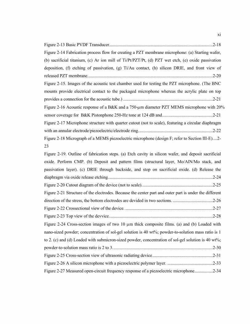
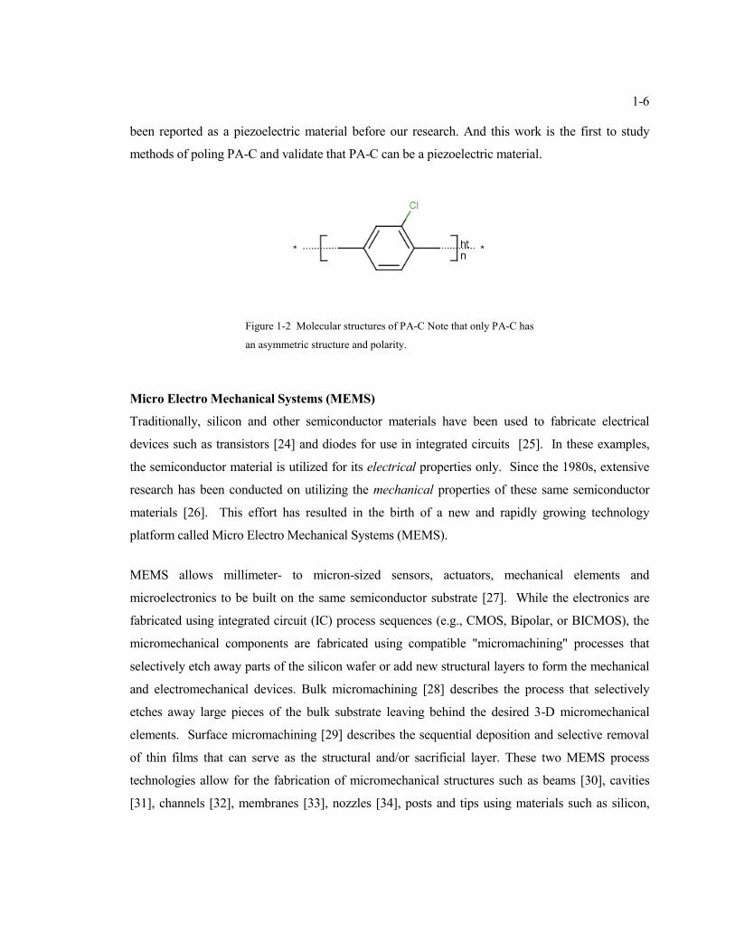
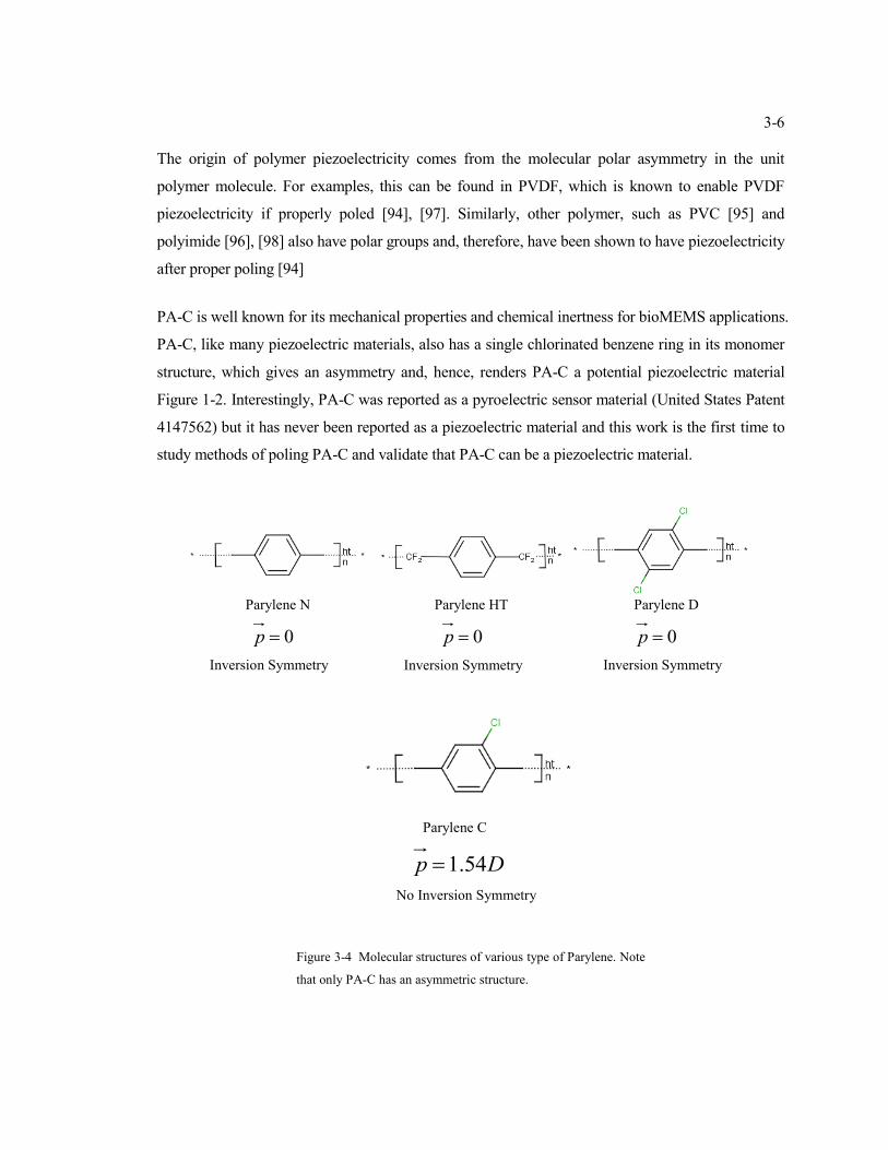
PA-C is well known for its mechanical properties and chemical inertness for bioMEMS applications.
PA-C, like many piezoelectric materials, also has a single chlorinated benzene ring, which gives an
asymmetry and, hence, is a potential piezoelectric material as shown in Figure 1-2. Interestingly,
PA-C was reported as a pyroelectric sensor material (United States Patent 4147562) but it has never
Page 23
1-6
been reported as a piezoelectric material before our research. And this work is the first to study
methods of poling PA-C and validate that PA-C can be a piezoelectric material.
Figure 1-2 Molecular structures of PA-C Note that only PA-C has
an asymmetric structure and polarity.
Micro Electro Mechanical Systems (MEMS)
Traditionally, silicon and other semiconductor materials have been used to fabricate electrical
devices such as transistors [24] and diodes for use in integrated circuits [25]. In these examples,
the semiconductor material is utilized for its electrical properties only. Since the 1980s, extensive
research has been conducted on utilizing the mechanical properties of these same semiconductor
materials [26]. This effort has resulted in the birth of a new and rapidly growing technology
platform called Micro Electro Mechanical Systems (MEMS).
MEMS allows millimeter- to micron-sized sensors, actuators, mechanical elements and
microelectronics to be built on the same semiconductor substrate [27]. While the electronics are
fabricated using integrated circuit (IC) process sequences (e.g., CMOS, Bipolar, or BICMOS), the
micromechanical components are fabricated using compatible "micromachining" processes that
selectively etch away parts of the silicon wafer or add new structural layers to form the mechanical
and electromechanical devices. Bulk micromachining [28] describes the process that selectively
etches away large pieces of the bulk substrate leaving behind the desired 3-D micromechanical
elements. Surface micromachining [29] describes the sequential deposition and selective removal
of thin films that can serve as the structural and/or sacrificial layer. These two MEMS process
technologies allow for the fabrication of micromechanical structures such as beams [30], cavities
[31], channels [32], membranes [33], nozzles [34], posts and tips using materials such as silicon,
Page 24
1-7
silicon dioxide, silicon nitride, polysilicon, various metals and other silicon derivatives. Together
with a host of new MEMS technologies such as LIGA [35], plastic injection molding [36],
microstereolithography [37], laser micromachining [38], micro electrical discharge machining [39],
silicon carbide processes [40] and selective Parylene deposition/etching [41], MEMS promises to
revolutionize nearly every product category by bringing together (silicon-based) microelectronics
with miniature sensor and actuator technology.
MEMS is truly an enabling technology allowing the development of smart products by augmenting
the computational ability of microelectronics with the perception and control capabilities of
microsensors and microactuators. For the first time in scientific history, this enables the creation of
sophisticated multifunctional microchips that can take input directly from their surrounding
environment through a MEMS microsensor (e.g., as sound, heat, moisture, pressure, etc.), process
the information through a microelectronic circuit, and relay a response back to the physical
environment through a MEMS microactuator (e.g., through force, magnetic field, etc.). The ideal
embodiment is for all of this to take place on the same microchip substrate.
Because MEMS devices are built with the same underlying technology and utilize the same
infrastructure as that used in the microelectronics industry, they can be effectively miniaturized and
mass-produced reliably and cost-efficiently. In the past decade, the United States Defense
Advanced Research Project Agency (DARPA) has poured millions of dollars into MEMS research.
Since the 1990s, the commercialization of MEMS devices has also developed at a torrid pace.
Today, almost all the accelerometers used in car airbag deployment systems are MEMS
accelerometers [42]. Many of the most precise pressure sensors used in portable devices are MEMS
pressure sensors [43]. Most recently, the biotech industry has embraced MEMS micro-fluidic
technology to develop microchip bioassays, gene screening and chemical analysis systems [44].
Booming communication infrastructure companies (such as Lucent Technologies Inc. and Nortel
Networks Corp.) are now turning to MEMS technology to develop micro-optical switches [45] that
will re-route the packets of light blazing down fiber optic cables around the globe. MEMS devices
are beginning to revolutionize the way we interact with our macroscopic and microscopic
environments.
Page 25
1-8
THESIS OUTLINE
The aim of this work is to develop miniature, inexpensive, high-quality, self-generating
piezoelectric microphones that can be fabricated using piezoelectric PA-C by Micro Electro
Mechanical systems (MEMS) technology. These MEMS piezoelectric microphones are to be used
in any application where a conventional piezoelectric and electret microphone can be used (such as
in cell phones, and hearing aids).
Although a complete piezoelectric PA-C MEMS microphone affords many advantages, there are
many components of the technology that need to be developed or refined before a fully functional
device was fabricated. With respect to the MEMS microphone history, theory, poling process,
design, modeling, fabrication, packaging, testing and performance specs, this thesis is organized as
follows:
Chapter 2 introduces piezoelectric materials and reviews discrete and MEMS piezoelectric
microphones.
Chapter 3 introduces the piezoelectric properties of poled Parylene-C. It includes the poling
process and characteristics of piezoelectric Parylene-C.
Chapter 4 provides the theory and history behind a piezoelectric circular diaphragm and the
design aspects of the microphones.
Chapter 5 details the fabrication, testing and analysis of piezoelectric Parylene-C MEMS
microphones.
Chapter 6 summarizes the entire thesis.
Page 27
2-1
C h a p t e r 2
PIEZOELECTRIC MICROPHONE REVIEW
Piezoelectricity
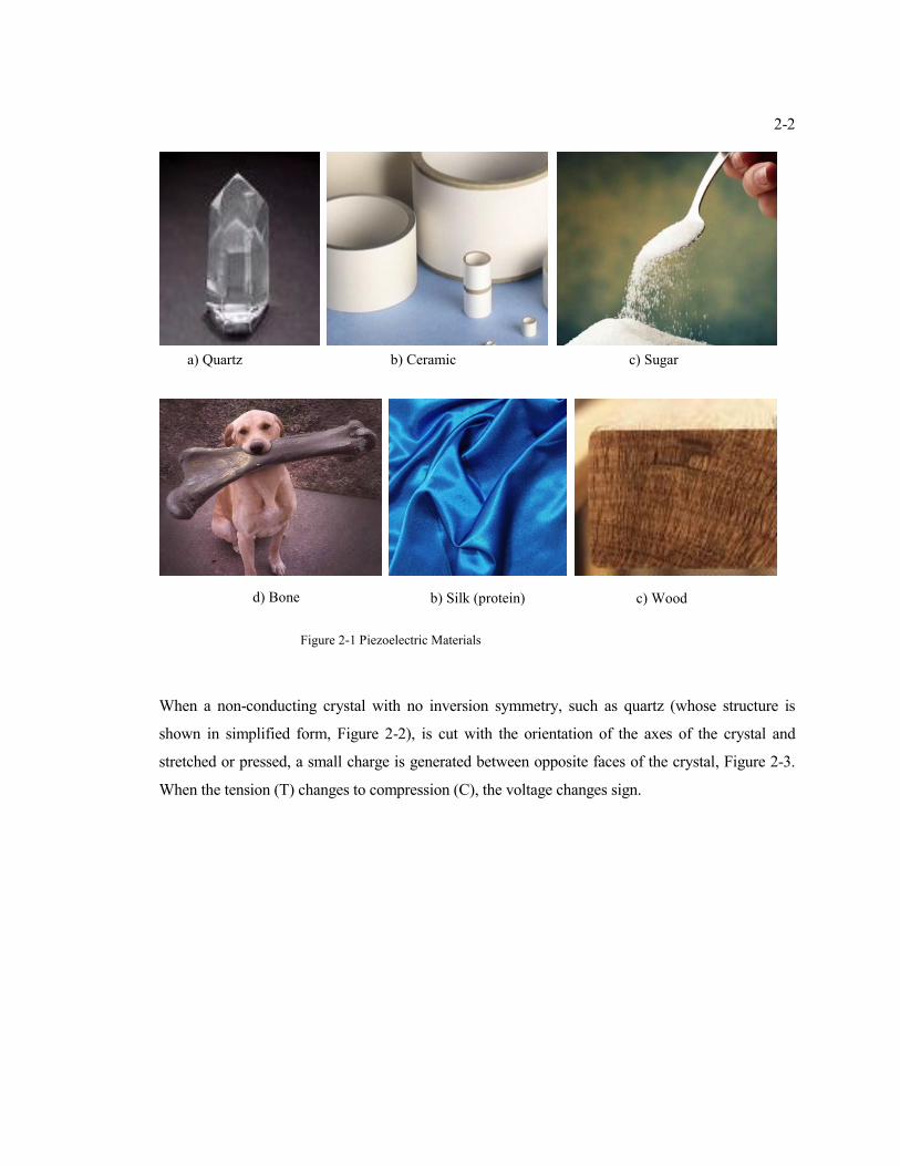
When the charge is generated in certain solid materials, (such as crystals like quartz topaz, or
ceramics, bone, protein, sugar and wood Figure 2-1), by applied mechanical stress, these materials
can be called as piezoelectric material. It is derived from the Greek piezo, which means to squeeze
or press, and electric, which stands for amber, an ancient source of electric charge.[46]
In 1820 Becquerel described and observed piezoelectric effects,[1] although a systematic study
leading to modern understanding of these effects is credited to the Curies.[2] The two physicists
found that the surfaces of certain crystals become electrically charged when the crystal is
mechanically loaded.
Page 28
2-2
Figure 2-1 Piezoelectric Materials
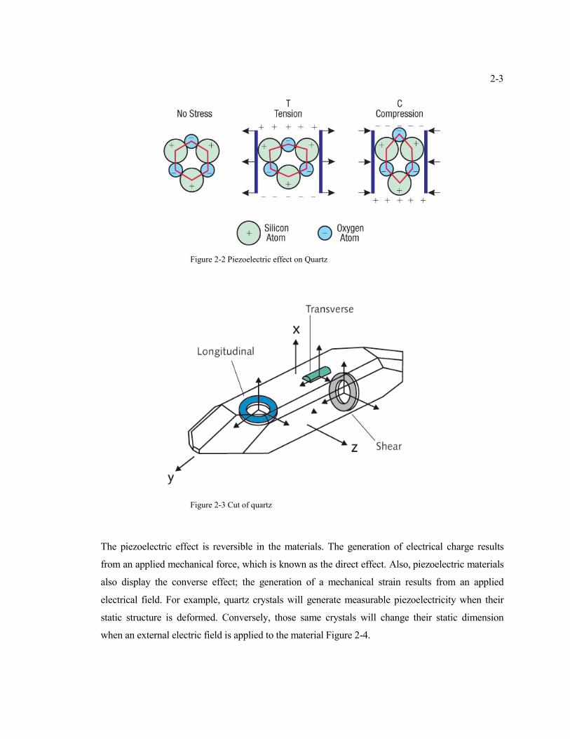
When a non-conducting crystal with no inversion symmetry, such as quartz (whose structure is
shown in simplified form, Figure 2-2), is cut with the orientation of the axes of the crystal and
stretched or pressed, a small charge is generated between opposite faces of the crystal, Figure 2-3.
When the tension (T) changes to compression (C), the voltage changes sign.
a) Quartz b) Ceramic c) Sugar
d) Bone b) Silk (protein) c) Wood
Page 29
2-3
Figure 2-2 Piezoelectric effect on Quartz
Figure 2-3 Cut of quartz
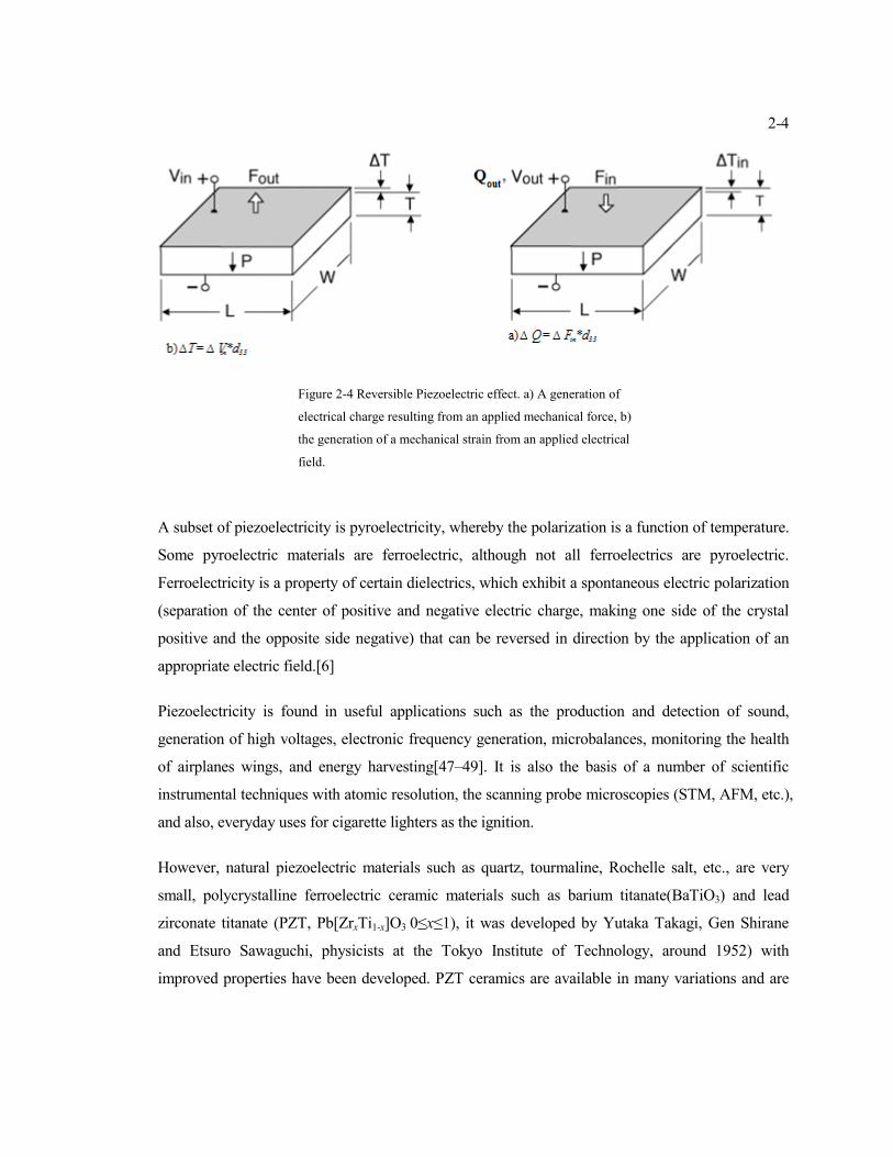
The piezoelectric effect is reversible in the materials. The generation of electrical charge results
from an applied mechanical force, which is known as the direct effect. Also, piezoelectric materials
also display the converse effect; the generation of a mechanical strain results from an applied
electrical field. For example, quartz crystals will generate measurable piezoelectricity when their
static structure is deformed. Conversely, those same crystals will change their static dimension
when an external electric field is applied to the material Figure 2-4.
Page 30
2-4
Figure 2-4 Reversible Piezoelectric effect. a) A generation of
electrical charge resulting from an applied mechanical force, b)
the generation of a mechanical strain from an applied electrical
field.
A subset of piezoelectricity is pyroelectricity, whereby the polarization is a function of temperature.
Some pyroelectric materials are ferroelectric, although not all ferroelectrics are pyroelectric.
Ferroelectricity is a property of certain dielectrics, which exhibit a spontaneous electric polarization
(separation of the center of positive and negative electric charge, making one side of the crystal
positive and the opposite side negative) that can be reversed in direction by the application of an
appropriate electric field.[6]
Piezoelectricity is found in useful applications such as the production and detection of sound,
generation of high voltages, electronic frequency generation, microbalances, monitoring the health
of airplanes wings, and energy harvesting[47–49]. It is also the basis of a number of scientific
instrumental techniques with atomic resolution, the scanning probe microscopies (STM, AFM, etc.),
and also, everyday uses for cigarette lighters as the ignition.
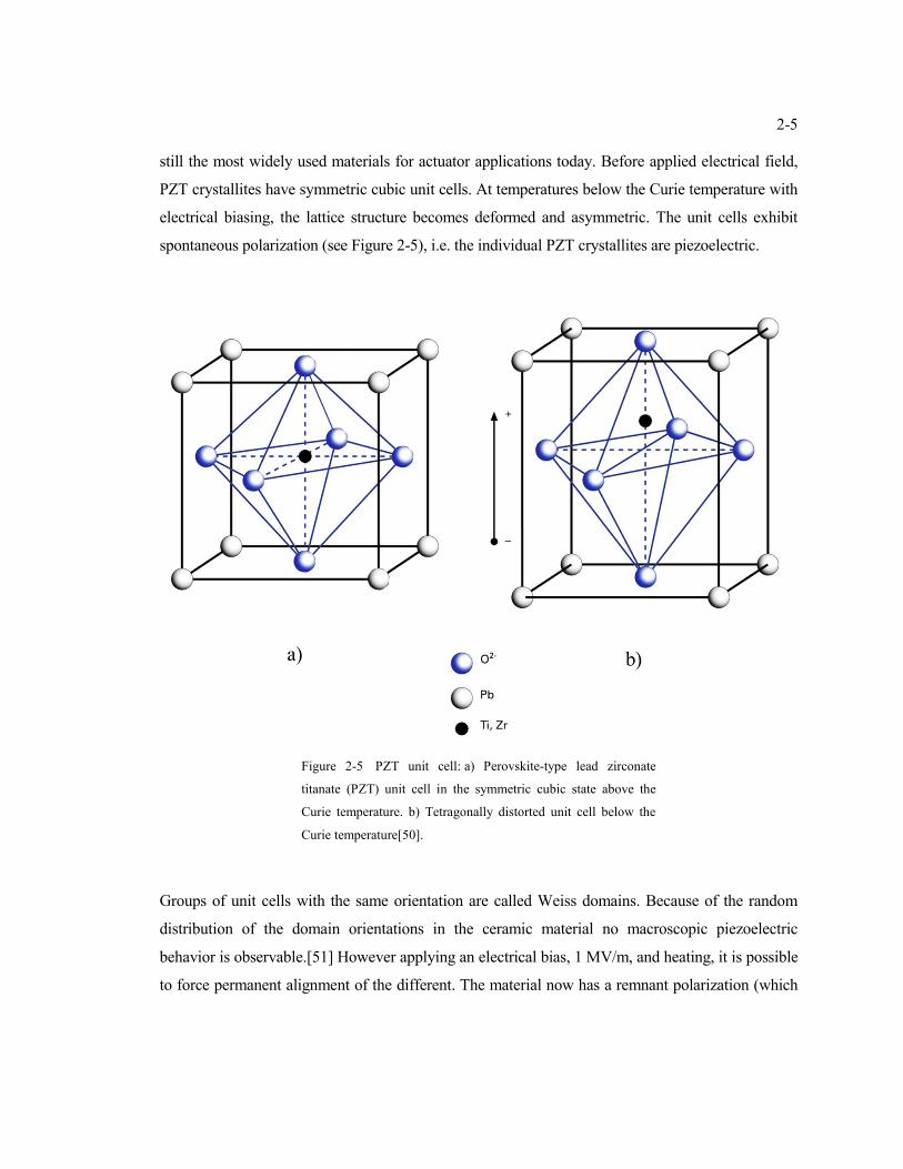
However, natural piezoelectric materials such as quartz, tourmaline, Rochelle salt, etc., are very
small, polycrystalline ferroelectric ceramic materials such as barium titanate(BaTiO3) and lead
zirconate titanate (PZT, Pb[ZrxTi1-x]O3 0≤x≤1), it was developed by Yutaka Takagi, Gen Shirane
and Etsuro Sawaguchi, physicists at the Tokyo Institute of Technology, around 1952) with
improved properties have been developed. PZT ceramics are available in many variations and are
Page 31
2-5
still the most widely used materials for actuator applications today. Before applied electrical field,
PZT crystallites have symmetric cubic unit cells. At temperatures below the Curie temperature with
electrical biasing, the lattice structure becomes deformed and asymmetric. The unit cells exhibit
spontaneous polarization (see Figure 2-5), i.e. the individual PZT crystallites are piezoelectric.
Figure 2-5 PZT unit cell: a) Perovskite-type lead zirconate
titanate (PZT) unit cell in the symmetric cubic state above the
Curie temperature. b) Tetragonally distorted unit cell below the
Curie temperature[50].
Groups of unit cells with the same orientation are called Weiss domains. Because of the random
distribution of the domain orientations in the ceramic material no macroscopic piezoelectric
behavior is observable.[51] However applying an electrical bias, 1 MV/m, and heating, it is possible
to force permanent alignment of the different. The material now has a remnant polarization (which
Page 32
2-6
can be degraded by exceeding the mechanical, thermal and electrical limits of the material)
properties as shown in Figure 2-6. Each arrow represents a polarization domain. The ceramic now
exhibits piezoelectric[50].
Figure 2-6 Electric dipoles in domains; a) unpoled ferroelectric
ceramic below curie temperature, b) during the poling (applying
electrical bias and heating near below the Curie temperature) and
c) after poling[50].
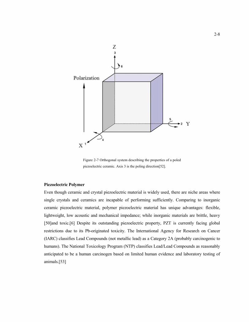
Definitions of Piezoelectric Coefficients and Directions
Because of the anisotropic nature of PZT ceramics, piezoelectric effects depend ondirection. To
identify directions, the axes 1, 2, and 3 will be introduced (corresponding to X, Y, Z of the classical
right-hand orthogonal axis set). The axes 4, 5 and 6 identify rotations (shear),θX, θY, θZ (also known
as U, V, W.) The axes and polarization are shown in Figure 2-7.
The direction of polarization (axis 3) is established during the poling process by a strong electrical
field applied between two electrodes. For linear actuator (translator) applications, the piezo
properties along the poling axis are the most important (largest deflection).
Page 33
2-7
Piezoelectric materials can be characterized by several coefficients: dij and gij.
1. Charge mode (dij), Strain coefficients [m/V] or charge output coefficients [C/N]: A strain
developed [m/m] per unit of electric field strength applied [V/m] or charge density developed
[C/m2] per given stress [N/m
2]. The charge output coefficients [C/N] is used to describe
mechanical input and electrical output, such as microphone and vibration sensor. Generally,
pC/N (pico-Coulomb per Newton) is widely used. The strain coefficient [m/V] is used for
describing electrical input and mechanical output (for example, buzzer element and precise
linear stage).
2. Voltage mode; gij: Voltage coefficients or field output coefficients [Vm/N, (V/m)/(N/m2)]:
Open-circuit electric field developed [V/m] per applied mechanical stress [N/m2] or strain
developed [m/m] per applied charge density [C/m2].
kij: Coupling coefficients [dimensionless]. The coefficients are energy ratios describing the
conversion from mechanical to electrical energy or vice versa. k2 is the ratio of energy stored
(mechanical or electrical) to energy (mechanical or electrical) applied.
2 electrical energy stored as mechanical energy
input electrical energyk
2 mechanical energy stored as electrical energy
input mechanical energyk
Page 34
2-8
Figure 2-7 Orthogonal system describing the properties of a poled
piezoelectric ceramic. Axis 3 is the poling direction[52].
Piezoelectric Polymer
Even though ceramic and crystal piezoelectric material is widely used, there are niche areas where
single crystals and ceramics are incapable of performing sufficiently. Comparing to inorganic
ceramic piezoelectric material, polymer piezoelectric material has unique advantages: flexible,
lightweight, low acoustic and mechanical impedance; while inorganic materials are brittle, heavy
[50]and toxic.[6] Despite its outstanding piezoelectric property, PZT is currently facing global
restrictions due to its Pb-originated toxicity. The International Agency for Research on Cancer
(IARC) classifies Lead Compounds (not metallic lead) as a Category 2A (probably carcinogenic to
humans). The National Toxicology Program (NTP) classifies Lead/Lead Compounds as reasonably
anticipated to be a human carcinogen based on limited human evidence and laboratory testing of
animals.[53]
Page 35
2-9
The piezoelectric strain constant (d33) for the polymer is lower (Poly-Vinyl DiFluoro , PVDF ,
30pC/N) than that of the ceramic (PZT, 300 pC/N). However, due to its low Young’s modulus,
piezoelectric polymers (PVDF, 240 mV-m/N) have much higher piezoelectric stress constants (g33)
than ceramic (PZT, 11 mV-m/N), which indicating that they can be better sensor than ceramics.
Piezoelectric polymeric sensors and actuators offer the advantage of processing flexibility because
they are lightweight, tough, readily manufactured into large areas, and can be cut and reformed into
complex shapes. Polymers also exhibit high strength and high impact resistance.[7] Other notable
features of polymers are low dielectric constant, low elastic stiffness, and low density, which result
in a high voltage sensitivity (excellent sensor characteristic), and low acoustic and mechanical
impedance (crucial for medical and underwater applications). Thus, for example, PVDF is widely
used as sensor material such as, traffic signal control loop sensor buried under the load, musical
instrument pickups, sports scoring, impact printers, bearing wear sensors, fan flow sensor and
accelerometers.[8] Polymers also typically possess a high dielectric breakdown and high operating
field strength, which means that they can withstand much higher driving fields than ceramics.
Polymers offer the ability to pattern electrodes on the film surface, and to pole only selected regions.
Based on these features, piezoelectric polymers earned their own area for technical applications and
useful device configurations. In MEMS field, curable polyimide is also used to build a touch sensor
array, air flow sensor and vibration sensor.[9–13]
For being Piezoelectric Polymers.
For respecting to polarization stability, four critical elements exist for all piezoelectric polymers,
regardless for both semicrystalline and amorphous polymers. As summarized by Broadhurst and
Davis[54] these four elements are: a) the permanent molecular dipoles; b) the molecular dipoles
aligning ability to external electrical field; c) the sustainability of the dipole alignment once it is
accomplished; and d) the durability to undergo large strains when mechanically stressed.
Page 36
2-10
Mechanism of piezoelectricity in semicrystalline polymers.
As we mention before, semicrystalline polymers must have a polar crystalline phase to be a
piezoelectric material. The crystallites disperse within amorphous regions of polymer as shown in
Figure 2-8. The amorphous region is related to a glass transition temperature which dominates the
mechanical properties of the polymer while the crystallites are related to a melting temperature that
decides the upper limit of the use temperature. The degree of crystallinity in polymers depends on
their thermal history and origin of preparation method.
Most semicrystalline polymers have several polymorphic phases, some of which may be polar.
Electrical poling is accomplished by applying an electric field across the thickness of the polymer as
depicted in Figure 2-8b). Typically an electric field on the order of 50 MV/m is sufficient to effect
crystalline orientation at 90~100oC.[52], [55–61] Either a direct contact method or a corona
discharge[62], [63] can be applied to Polymer poling. Also, it is reported that the simultaneous
stretching of a polymer film while the poling process can increase piezoelectric coefficient roughly
2 times, Figure 2-8c).[64] Depending on whether stretching is uniaxial or biaxial, the electrical and
mechanical properties (and therefore the transduction response), are either highly anisotropic
(d31≠d32) or isotropic (d31=d32) in the plane of the polymer sheet.
The corona charge is favorable for manufacture commercially available poly-vinylidene fluoride
(PVDF) film because it doesn’t require contacting electrodes and large area samples can be poled in
a continuous extrusion. For semicrystalline polymers the amorphous phase supports the crystal
orientation and the polarization is stable up to the Curie temperature. This polarization can remain
constant for many years if it is not influenced by the spurious effects of moisture uptake or elevated
temperatures.
Page 37
2-11
Figure 2-8 Schematic illustration showing random stacks of
amorphous and crystal lamellae in PVDF polymer.
Poly-Vinyl DiFluoro (PVDF).
Interest in the electrical properties of PVDF began in 1969 when Kawai [65] showed that thin films
that had been poled exhibited a very large piezoelectric coefficient, 6-7 pC/N, a value which is
about ten times larger than had been observed in any other polymer. PVDF is inherently polar. The
spatially symmetrical disposition of the hydrogen and fluorine atoms along the polymer chain gives
rise to unique polarity effects that influence the electromechanical response, solubility, dielectric
properties, crystal morphology and yield an unusually high dielectric constant. The dielectric
constant of PVDF is about 12, which is four times greater than most polymers. This makes PVDF
attractive for integration into devices as the signal to noise ratio is less for higher dielectric materials.
The amorphous phase in PVDF has a glass transition point (-35oC) that is well below room
temperature, hence the material is quite flexible and readily strained at room temperature. PVDF is
typically 50 to 60% crystalline depending on thermal and processing history and has at least four
crystal phases (α, β, γ, and δ), of which at least three are polar.[66–69] The most stable, non-polar
phase results upon casting PVDF from the melt and can be transformed into the polar phase by
Page 38
2-12
mechanically stretching at elevated temperatures or into the polar phase by rotating the molecular
chain axis with a high electric field (~130 MV/m) [70]. The phase is most important for
piezoelectric considerations and has a dipole moment perpendicular to the chain axis of 2.1 D
corresponding to a dipole concentration. After poling PVDF, the room temperature polarization
stability is excellent; however polarization and piezoelectricity degrade with increasing temperature
and is erased at its Curie temperature. Previously it was believed that polarization stability was
defined only by the melting temperature of the PVDF crystals. Recently, some researchers suggest
that the polarization stability of PVDF and its co-polymers is associated with Coulomb interactions
between injected, trapped charges and oriented dipoles in the crystals.[71] They hypothesize that the
thermal decay of the polarization is caused by the thermally activated removal of the trapped
charges from the traps at the surface of the crystals. The role of trapped charges in stabilizing
orientation in both semicrystalline and amorphous polymers is still a subject that needs further
study.[64]
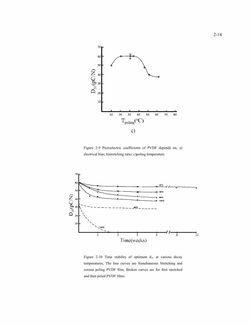
A simultaneous stretching and corona poling process is studied for PVDF.[64] Without the
stretching d31 is around 30 pC/N. But as we see in Figure 2-9a) it becomes around 60 pC/N. Also,
poling condition is studied and it shows saturation over poling electrical field beyond 50 Mv/m
from Figure 2-9a). This is due to saturation in the number of crystallites and/or dipoles aligned in
the field direction. For the stretching ratio as shown in Figure 2-9b), the maximum d31 is obtained
at the ratio is 4.5. The stretching ratio is defined as the final length over initial length. From Figure
2-9c), we can see the d31 against poling temperature Tpoling. d31 increases with poling temperature to
a maximum of 60 pC/N in the range 70-85 oC, and decreases to 37 pC/N when poled at 110
oC. The
drop in d31 may be due to an increase in electrical conductivity, which would reduce the effective
poling field. The optimum poling parameters obtained from Figure 2-9 are Epoling = 55 MV/m,
Stretching Ratio = 4.5 and Tpoling =80oC.
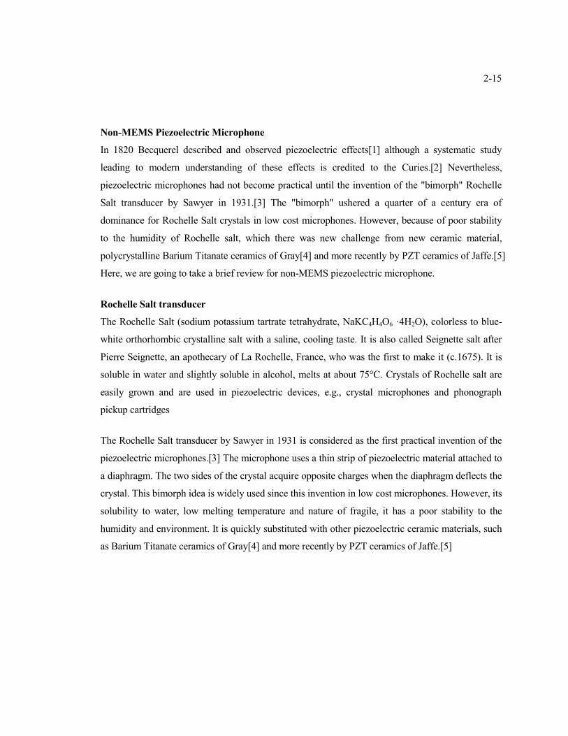
The film at the optimum condition is also tested for its stability against the time and temperature as
shown is Figure 2-10.
Page 40
2-14
Figure 2-9 Piezoelectric coefficients of PVDF depends on, a)
electrical bias; b)stretching ratio; c)poling temperature.
Figure 2-10 Time stability of optimum d31 at various decay
temperatures, The line curves are Simultaneous Stretching and
corona poling PVDF film; Broken curves are for first stretched
and then poled PVDF films.
Page 41
2-15
Non-MEMS Piezoelectric Microphone
In 1820 Becquerel described and observed piezoelectric effects[1] although a systematic study
leading to modern understanding of these effects is credited to the Curies.[2] Nevertheless,
piezoelectric microphones had not become practical until the invention of the "bimorph" Rochelle
Salt transducer by Sawyer in 1931.[3] The "bimorph" ushered a quarter of a century era of
dominance for Rochelle Salt crystals in low cost microphones. However, because of poor stability
to the humidity of Rochelle salt, which there was new challenge from new ceramic material,
polycrystalline Barium Titanate ceramics of Gray[4] and more recently by PZT ceramics of Jaffe.[5]
Here, we are going to take a brief review for non-MEMS piezoelectric microphone.
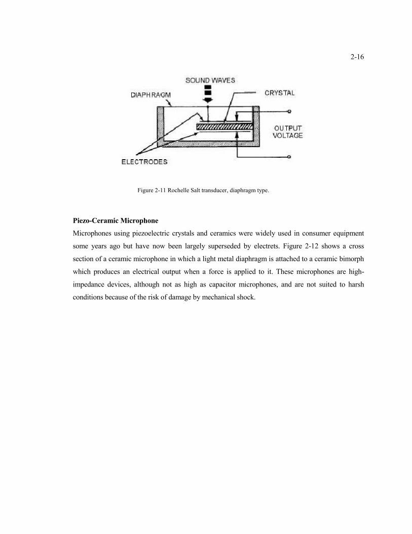
Rochelle Salt transducer
The Rochelle Salt (sodium potassium tartrate tetrahydrate, NaKC4H4O6 ·4H2O), colorless to blue-
white orthorhombic crystalline salt with a saline, cooling taste. It is also called Seignette salt after
Pierre Seignette, an apothecary of La Rochelle, France, who was the first to make it (c.1675). It is
soluble in water and slightly soluble in alcohol, melts at about 75°C. Crystals of Rochelle salt are
easily grown and are used in piezoelectric devices, e.g., crystal microphones and phonograph
pickup cartridges
The Rochelle Salt transducer by Sawyer in 1931 is considered as the first practical invention of the
piezoelectric microphones.[3] The microphone uses a thin strip of piezoelectric material attached to
a diaphragm. The two sides of the crystal acquire opposite charges when the diaphragm deflects the
crystal. This bimorph idea is widely used since this invention in low cost microphones. However, its
solubility to water, low melting temperature and nature of fragile, it has a poor stability to the
humidity and environment. It is quickly substituted with other piezoelectric ceramic materials, such
as Barium Titanate ceramics of Gray[4] and more recently by PZT ceramics of Jaffe.[5]
Page 42
2-16
Figure 2-11 Rochelle Salt transducer, diaphragm type.
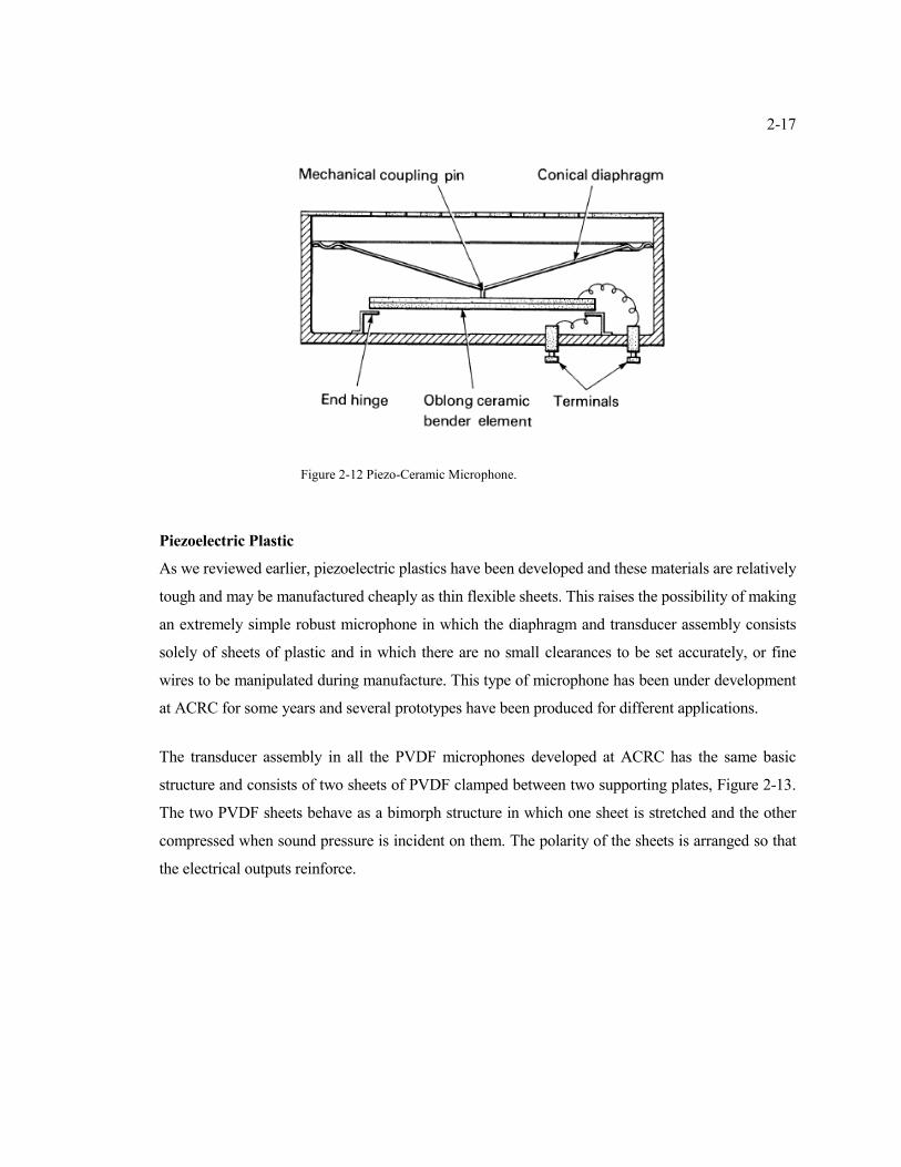
Piezo-Ceramic Microphone
Microphones using piezoelectric crystals and ceramics were widely used in consumer equipment
some years ago but have now been largely superseded by electrets. Figure 2-12 shows a cross
section of a ceramic microphone in which a light metal diaphragm is attached to a ceramic bimorph
which produces an electrical output when a force is applied to it. These microphones are high-
impedance devices, although not as high as capacitor microphones, and are not suited to harsh
conditions because of the risk of damage by mechanical shock.
Page 43
2-17
Figure 2-12 Piezo-Ceramic Microphone.
Piezoelectric Plastic
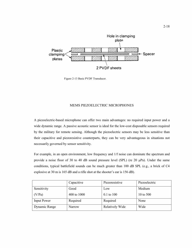
As we reviewed earlier, piezoelectric plastics have been developed and these materials are relatively
tough and may be manufactured cheaply as thin flexible sheets. This raises the possibility of making
an extremely simple robust microphone in which the diaphragm and transducer assembly consists
solely of sheets of plastic and in which there are no small clearances to be set accurately, or fine
wires to be manipulated during manufacture. This type of microphone has been under development
at ACRC for some years and several prototypes have been produced for different applications.
The transducer assembly in all the PVDF microphones developed at ACRC has the same basic
structure and consists of two sheets of PVDF clamped between two supporting plates, Figure 2-13.
The two PVDF sheets behave as a bimorph structure in which one sheet is stretched and the other
compressed when sound pressure is incident on them. The polarity of the sheets is arranged so that
the electrical outputs reinforce.
Page 44
2-18
Figure 2-13 Basic PVDF Transducer.
MEMS PIEZOELECTRIC MICROPHONES
A piezoelectric-based microphone can offer two main advantages: no required input power and a
wide dynamic range. A passive acoustic sensor is ideal for the low-cost disposable sensors required
by the military for remote sensing. Although the piezoelectric sensors may be less sensitive than
their capacitive and piezoresistive counterparts, they can be very advantageous in situations not
necessarily governed by sensor sensitivity.
For example, in an open environment, low frequency and 1/f noise can dominate the spectrum and
provide a noise floor of 30 to 40 dB sound pressure level (SPL) (re 20 μPa). Under the same
conditions, typical battlefield sounds can be much greater than 100 dB SPL (e.g., a brick of C4
explosive at 30 m is 165 dB and a rifle shot at the shooter’s ear is 156 dB).
Capacitive Piezoresistive Piezoelectric
Sensitivity
(V/Pa)
Good
400 to 1000
Low
0.1 to 100
Medium
10 to 500
Input Power Required Required None
Dynamic Range Narrow Relatively Wide Wide
Page 45
2-19
For a passive piezoelectric microphone, there are several options for the thin film sensor material
including ZnO, aluminum nitride (AlN), and lead zirconate titanate (PZT).
A piezoelectric microphone based on PZT thin films[72]
Polcawich, Ronald G et. al. developed a piezoelectric microphone based on PZT thin films in order
to investigate its potential use as a passive sensing element in a photoacoustic resonant cell.[72] The
microphone fabrication process began with a double-side polished silicon wafer and used several
different types of deposition systems. A plasma-enhanced chemical vapor-deposited (PECVD)
silicon dioxide thin film (1 m thick) was deposited with a Plasma-Therm 790 reactor using a
mixture of SiH4, He, and N2O. The oxide served as the membrane structural layer and was chosen
to be 1 m thick. After the deposition, the film was annealed in an A.G. Associates Heatpulse 610
rapid thermal anneal (RTA) furnace at 700 °C for 60 seconds in a nitrogen atmosphere to remove
the trapped hydrogen within the film. And this annealing caused the film to obtain a slightly tensile
stress, for producing a planar membrane.
After the oxide was deposited and annealed, a metal electrode was deposited via sputtering to serve
as the bottom electrode and as a growth template for the piezoelectric actuator. Titanium/Platinium
(200/800 Å ) was sputtered in a Varian 3190 direct current (DC) magnetron sputter deposition
system. Titanium layer is used for improving adhesion. Following the platinum deposition, the
wafers were annealed in the RTA furnace at 700 °C for 60 seconds in a flowing dry air in order to
improve the adhesion between the oxide and metal layers and the surface texture of the platinum
before deposition of the piezoelectric thin film.
The next fabrication step was to deposit the PbZr0.52Ti0.48O3 thin film. The building process was a
sol-gel spin-on process. First, a PZT sol-gel solution was prepared via a modified alkoxide process
first introduced by Budd, Dey, and Payne [73]. This process used lead acetate trihydrate, zirconium
n-propoxide, and titanium isopropoxide as the precursors and 2-methoxyethanol as the solvent.
Once the sol-gel solution was prepared and aged, the repetitive deposition process, as depicted in
Figure 2-14 c), began with a portion of the sol dispensed onto a platinized silicon substrate. The
wafer was then spun at 2,500 rpm for 30 seconds. Next, the wafers were placed onto a hotplate at
Page 46
2-20
350 °C for 120 seconds causing the film to undergo the pyrolysis, which thereby decomposed all
the organics. This process of deposition, spin, and pyrolysis was then repeated a total of four times.
After the last pyrolysis, the wafer was annealed in a RTA furnace at 700 °C for 30 seconds in the
flowing air in order to crystallize the PZT thin film. The result was approximately a 0.25 m PZT
film, and the entire process was continued in order to achieve the desired thickness of a 1-m PZT
thin film. After the piezoelectric was deposited, a top electrode of platinum (800 Å ) was sputter
deposited onto the wafer surface. The wafers were then annealed in an RTA at 350 °C for 120
seconds in the flowing air to improve adhesion and reduce any sputtering-induced surface damage.
The resultant wafer stack at this stage was Si/SiO2/Ti/Pt/PZT/Pt.
Figure 2-14 Fabrication process flow for creating a PZT
membrane microphone: (a) Starting wafer, (b) sacrificial titanium,
(c) Ar ion mill of Ti/Pt/PZT/Pt, (d) PZT wet etch, (e) oxide
passivation deposition, (f) etching of passivation, (g) Ti/Au
contact, (h) silicon DRIE, and front view of released PZT
membrane.
Page 47
2-21
Figure 2-15. Images of the acoustic test chamber used for testing
the PZT microphone. (The BNC mounts provide electrical contact
to the packaged microphone whereas the acrylic plate on top
provides a connection for the acoustic tube.)
Figure 2-16 Acoustic response of a B&K and a 750-m diameter
PZT MEMS microphone with 20% sensor coverage for B&K
Pistonphone 250-Hz tone at 124 dB and
Page 48
2-22
An AlN MEMS Piezoelectric Microphone for Aeroacoustic Applications[74]
Achieving a high-dynamic range, particularly a high pmax, is the most difficult performance
challenge for an audio-band aeroacoustic microphone. Until recently, difficulties in fabrication and
limited commercial availability of aluminum nitride (AlN) films resulted in very little attention to
this material for use in microfabricated microphones[75–77], despite its attractive properties. These
include high stiffness, a high material figure of merit for sensitivity (g31), low dielectric loss, and
high intrinsic signal-to-noise ratio [78]. For the fuselage array application, the low dielectric loss of
AlN is a critical advantage over PZT and ZnO because it translates to an improved low-frequency
microphone response.[78] As a result, AlN is utilized in this work.
Figure 2-17 Microphone structure with quarter cutout (not to
scale), featuring a circular diaphragm with an annular
electrode/piezoelectric/electrode ring.
A depiction (not scaled exactly) of the microphone structure enabled by this process is shown in
Figure 2-17. The operation of the microphone is based on deflection of the circular diaphragm due
to an incident acoustic pressure wave. The annular metal/piezoelectric/metal film stack situated on
the high stress/strain region around the outer boundary of the diaphragm produces a proportional
output voltage. The diaphragm is composed of passivation, electrode (molybdenum), piezoelectric
Page 49
2-23
(aluminum nitride), and structural layers. As proprietary features of the FBAR-variant process, the
materials used in the passivation and structural layers are not disclosed.
Exact FBAR process details are proprietary. However, a general outline of fabrication steps was
published by Avago Technologies[75],[79] and is summarized in Fig. 3. The process involved both
surface and bulk micromachining, starting with a 675-m-thick 150-mm (6-in) silicon wafer. First,
a shallow cavity was etched and filled with sacrificial material, which served to define the
diaphragm diameter and set an etch stop for subsequent backside processing. The wafer surface was
thinned to 500 m and planarized via chemical–mechanical polishing (CMP), as in Figure 2-19a).
The structural, metal, piezoelectric, and passivation layers, in addition to the bond pads, were then
deposited and patterned in a set of proprietary process steps [Figure 2-19b)]. A deep reactive ion
etch (DRIE) from the backside of the wafer formed the back cavity [Figure 2-19c)], and the
sacrificial material was etched to release the diaphragm [Figure 2-19d)]. A fabricated and diced
microphone is shown in Figure 2-18.
Figure 2-18 Micrograph of a MEMS piezoelectric microphone
(design F; refer to Section III-E).
Page 50
2-24
Figure 2-19. Outline of fabrication steps. (a) Etch cavity in silicon
wafer, and deposit sacrificial oxide. Perform CMP. (b) Deposit
and pattern films (structural layer, Mo/AlN/Mo stack, and
passivation layer). (c) DRIE through backside, and stop on
sacrificial oxide. (d) Release the diaphragm via oxide release
etching.
The performance of microphones with thin-film diaphragms is extremely sensitive to film stress.
The amount of stress control varies by process; sputter deposition (common for AlN), for instance,
is a complex process that does afford some flexibility to tailor stresses. Customization of the stress
state is achieved via adjustment of bias power, argon pressure, sputtering gas mass, temperature,
and/or deposition rate.[80] Avago Technologies is able to adjust film deposition parameters to
target a large range of film stresses.
Page 51
2-25
ZnO on Si integrated acoustic sensor[81]
The structure of the device is based upon a ZnO PIFET[82]. A thin ZnO piezoelectric film is
connected to the gate of an MOS amplifier integrated on the same Si substrate. When a
piezoelectric voltage is created across the ZnO layer, it modulates the input signal to the gate of the
MOS, varying the channel current. In order to extend the frequency response of the devices to
below 1 Hz, insulating layers of SiOx are used to encapsulate the ZnO film, the sensor electrodes
and the connecting leads to the MOS amplifier. This effectively reduces surface and interface
charge leakages.[83] The acoustic sensor design is shown in Figure 2-20. A thin diaphragm is
formed under the ZnO active film using anisotropic etching techniques, giving the device a high
sensitivity to incoming sound waves. The concentric electrode configuration, shown in Figure 2-21,
was designed to cancel the sensor response to temperature variations due to the pyroelectric
property of the ZnO.[84] This is an important concern, especially for low-frequency applications.
The electrode pattern forms two ZnO capacitors, one formed by the center electrode, the other by
the outer ring electrode. These two capacitors are connected in series through the top circular
electrode and the output signal is taken across the bottom concentric electrodes. The
pyroelectrically induced charges being uniform in the whole ZnO film.
Figure 2-20 Cutout diagram of the device (not to scale).
Page 52
2-26
Figure 2-21 Structure of the electrodes. Because the center part
and outer part is under the different direction of the stress, the
bottom electrodes are devided in two sections.
On the other hand, when the diaphragm is flexed under a uniform pressure, the central part of the
diaphragm is under tension while the outer part is under compression, creating piezoelectric
voltages of opposite signs m the two capacitors. The piezoelectric signals add to one another, thus
increasing the pressure sensitivity of the device. A third advantage of this electrode design is that it
allows the connections between sensor and on-chip electronics to be made at the ZnO/Si interface,
suppressing step coverage problems. The structure dimensions are shown in Figure 2-22.
Page 53
2-27
Figure 2-22 Crossectional view of the device.
Using the stress equations of a circular plate with clamped edges [85], the device performances can
be computed. The expected sensitivity for a 3 mm diameter, 30 m thick diaphragm with a 3 m
thick ZnO layer is 37 uV/ubar Some noise computations were also conducted using a circuit
analysis program and these predicted a signal-to-noise ratio of 8:1 at 2 ubar.
The first step in the sensor fabrication is the processing of the amplifiers. These are PMOS devices
with a high input impedance (>1013
) The expected gain of amplification was 2 and the drain current
at standby was 10 pA with a 4 volt supply. After the SiO, layers and the bottom electrodes are
deposited, the ZnO process takes place. A planar magnetron sputtering system with a ZnO target
was used for the ZnO deposition. The film quality is very dependent on the careful adjustment of
the sputtering parameters.[86] Extensive development work was conducted to establish a process
yielding good quality ZnO layers with high piezoelectric efficiency and low stress levels. This is
particularly important m this sensor, since the diaphragm thicknesses are about 30 m while the
ZnO layer thickness is up to 5 m, any significant amount of thermal mismatch between the ZnO
layer and the substrate will result in unacceptable warpage of the diaphragm. After completion of
the front side processing, the diaphragms are etched from the back surface of the chips. The present
chip size is 6 mm on the side with a diaphragm diameter of 3 mm. The chip is shown m Figure 2-23.
Page 54
2-28
Figure 2-23 Top view of the devvice.
Fabrication and Characterization of Piezoelectric Micromachined Ultrasonic Transducers
with Thick Composite PZT Films[87]
This device is not a microphone but ultrasound-radiating applications. For the sound radiating,
thicker PZT films are preferred because generative force and response speed of the diaphragm-type
transducers increase with increasing film thickness. However, integration of 4 to 20um thick PZT
films on silicon wafer, either the deposition or the patterning, is still a bottleneck in the
micromachining process.
This research reports on a diaphragm type piezoelectric micromachined ultrasonic transducers. A
composite coating technique based on chemical solution deposition and high-energy ball milled
powder has been used to fabricate thick PZT films. The fabricated device with crack-free PZT films
up to 7 m thick was evaluated as an ultrasonic transmitter. The generated sound pressure level of
up to 120 dB indicates that the fabricated device has very good ultrasound-radiating performance
and, therefore, can be used to compose form of arrays for generating ultrasound beam with high
directivity in numerous applications.
Page 55
2-29
The key technique of the composite processing is how to prepare uniform slurry by dispersing PZT
powder (APC 850 from APC International Ltd., Mackeyville, PA) with desired size into PZT sol-
gel precursor solution (Zr/Ti = 53/47). The details of the slurry preparation have been described
elsewhere[88], [89]. High energy ball milling, which is effective in getting the well-dispersed slurry,
was used to perform the mixing procedure. A selected dispersant first was added to the powder
during ball milling to get surface-modified powder with desired size.
The smaller the powder is, the more important this procedure is. Afterward, the PZT sol-gel
solution was mixed with the surface-modified powders and ball milled till uniform slurry was
obtained. The prepared slurry then was deposited on platinized silicon wafer using a spin-coater.
The added powder can reduce the stress within the film significantly, thus it is easy to obtain thick
films without crack. During spin-coating, the important procedure is that powder-free, sol-gel thin
layers and slurry-derived thick layers were deposited alternately.
The first layer of powder-free thin film was deposited on the bottom electrode as a buffer layer to
enhance the adhesion between thick film and the substrate. After several thick coatings were
deposited, an intermediate pure precursor solution layer was deposited because it can infiltrate into
the pores or other defects in the thick film to increase the film density and smooth the film surface.
Figure 2-24 shows two typical microstructures of two composite films using nano-sized and
submicron-sized PZT powder, respectively.
Page 56
2-30
Figure 2-24 Cross-section images of two 10 m thick composite
films. (a) and (b) Loaded with nano-sized powder; concentration
of sol-gel solution is 40 wt%; powder-to-solution mass ratio is 1
to 2. (c) and (d) Loaded with submicron-sized powder,
concentration of sol-gel solution is 40 wt%; powder-to-solution
mass ratio is 2 to 3.
Page 57
2-31
Figure 2-25 Cross-section view of ultrasonic radiating device
First, a 1.8-m thick layer of thermal silicon oxide, which can be used as a structural layer of the
diaphragm, was grown on double side, polished silicon or SOI wafer, shown in Figure 2-25 a); a
silicon nitride layer with a thickness of 200 nm then was deposited as wet etch mask of backside
silicon (Si); after that, a lower temperature oxide (LTO) layer with a thickness of 350 nm was
deposited to enhance the reliability and heat resistance of the bottom electrode; a Ti/Pt layer, 200-
300 nm thick, was sputtered and patterned by using lift-off as a bottom electrode. The thick PZT
layers with required thickness then were deposited by using the composite technique. After a wet
etching of the PZT layer, a polyimide layer was spin-coated and patterned as an insulation layer to
minimize a parasitic capacitance induced by patterned electrode wiring. The top electrode also was
patterned by lift-off. And, the backside silicon was etched off by KOH or DRIE until the required
Page 58
2-32
thickness, usually within the range of 0 to 20 m, depending on each other with the thickness of the
PZT layer. In the example shown in Figure 2-25c), the PZT layer is about 3.5 m in thickness, the
backside silicon was completely etched out and only silicon oxide (SiO2) layer with a thickness of
about 2 m was left, the SiN/LTO is invisible because their thickness is too thin to be observed in
this magnification. If a SOI wafer with 20 m thick top silicon layer is used, the thickness of the
PZT layer should be about 10 m, or about half of the silicon layer thickness.
Electroacoustical measurements of silicon microphones on wafer scale[90]
A schematic view of the piezoelectric microphone is shown in Figure 2-26. The sensor consists of
an SiN/Al membrane (the aluminum metallization acts as one single bottom electrode), covered
with a thin polymer layer of (PVDF/ TrFE) and a top electrode split into two separate parts. In case
of a deflection of the membrane an electrical voltage between the top and the bottom electrode is
generated due to the transversal piezoelectric effect of the corona poled polymer. The voltages,
which are generated at the inner and outer part of the top electrode, are connected in series by the
bottom electrode, increasing the sensitivity of the microphone. The area of the membrane is about 1
mm2 and the source impedance amounts to 10-20 pF, depending on the thickness of the polymer
layer.
Page 59
2-33
Figure 2-26 A silicon microphone with a piezoelectric polymer
layer.
A measured open-circuit frequency response of a piezoelectric microphone (polymer thickness: 4.3
mm, membrane thickness: approximately 300 nm, polarization field about 150 MV/m), is shown in
Figure 2-27. The measured frequency response is flat within 61 dB between 100 Hz and 10 kHz
with a slight increase of 3 dB between 10 and 15 kHz. This increase may be due to a resonance of
the microphone above 20 kHz. The measured sensitivity to airborne sound at 1 kHz is 0.21 mV/Pa
(73.6 dB re: 1 V/Pa) and the loading amounts to -11 dB. Using these two values, an open-circuit
sensitivity of 0.74 mV/Pa (-62.6 dB re: 1 V/Pa) is measured.
Page 60
2-34
Figure 2-27 Measured open-circuit frequency response of a
piezoelectric microphone.
Microphone based on Polyvinylidene Fluoride (PVDF) micro-pillars and patterned
electrodes[91]
A sensor design consisting of micron-sized Polyvinylidene Fluoride (PVDF) pillars which generate
a charge when subjected to normal stresses associated with acoustic waves. A rigid membrane
placed between the micro-pillars and the acoustic medium ensures high mechanical coupling. The
electrode covering the micro-pillars is patterned to decrease the capacitance, and hence increase the
sensitivity of the sensor.
Page 61
2-35
Figure 2-28 Schematic of PVDF microphone process
Figure 2-29 Pillar structure formed from PVDF and corresponding
electrodes
PVDF micro-structures were fabricated using a procedure which is described in detail
elsewhere[92]. Previously patterned PDMS (polydimethylsiloxane) stamps molded from
Page 62
2-36
photolithographically fabricated masters were used to obtain arrays of PVDF micro-pillars with
designed dimensions (Figure 2-30).
A 10% PVDF solution in dimethylacetamide/acetone was spin coated on the PDMS stamps at
1000-2000 rpm for 1 min. The stamps were placed on a hot plate at 100 0C for 5 min in order to
drive off residual solvent and anneal the PVDF. The spin coated PVDF film was then transferred
onto the adhesive side of copper tape using slight pressure. Figure 2-29 shows scanning electron
micrographs of PVDF pillars.
Figure 2-30 Schematic diagram of PVDF micro-pillar sensor with
full electrodes.
Preliminary experiments were conducted with the goal to characterize the piezoelectric response of
the PVDF micro-pillars. These proof-of-concept experiments were conducted on a non-optimal
micro-pillar array (d = 5 m, g = 5 m, h = 6 m, N = M = 1000). A gold-coated glass slide was
placed on top of the micro-pillars (top electrode), and an electric field of ∼120MV/m was applied
across the electrodes (top positive and bottom negative) at 160 ◦ C for 3 h, and then at room
temperature for an additional hour to pole the PVDF micro-structures.
Page 63
2-37
Piezoelectric Polyimide MEMS Device[13]
The temperature stability of the piezoelectric properties of PVDF are maintained is limited to less
than 80 °C. In this research, a surface-micromachined process for fabricating the structural
components for polyimide-based MEMS with high-temperature stability is presented. The high
temperature performance of these modified polyimide films allows these films to maintain their
piezoelectric properties at temperatures up to 150 °C, twice that of PVDF[10–12], see the graph in
Figure 2-31.
Figure 2-31 The piezoelectric strain coefficient (actuator response)
of polyimides vs. PVDF.
Polyimide polymers have exceptional thermal, mechanical, and dielectric properties, polyimides are
already widely utilized as matrix materials in aircraft and as dielectrics in the microelectronics
industry. Recently, amorphous polyimides containing polar functional groups have been
synthesized and investigated at VCU and NASA LaRC for potential use as high temperature
piezoelectric sensors.[15][14]
Page 64
2-38
One special step of this device is, in order to keep the polyimide film preparation temperatures low
(to keep the underlying sacrificial photoresist intact), they used a chemically pre-imidized
polyimide solution for this process. In this case, to form the polyimid film, the solvents are
completely driven out using a 24-hour bake at 90 °C. Differential Scanning Calorimetry (DSC)
measurements are underway to verify that the films are completely cured.
Figure 2-32 Piezoelectric polyimide sensor structure.
To ensure that the suspended components do not contact with the substrate by capillary action
during drying, becoming permanently adhered by van der Waals forces. This is prevented in the
release process by replacing the acetone with methanol, which is then replaced with pentane and
finally, hexane. The wafer can then be dried in air at room temperature.
After the fabrication steps, poling step to orient the dipoles and give the polyimide film its
piezoelectric properties is accomplished by applying a voltage across the structure at an elevated
temperature (T>Tg). In this step, 100V is applied (applied between the upper and lower electrodes)
for 1.3 μm and 2.15 μm thick polyimide bridge structures (77 MV/m and 47 MV/m respectively) at
temperatures of 170 °C and 200 °C.
Page 65
2-39
MEMS Condenser Microphone
A condenser microphone has a high sensitivity and a wider bandwidth among the current
microphone technologies. Consequently, numerous researches have been accomplished to build a
MEMS condenser (electret) microphone.
In 1986, Hohm presented a MEMS condenser microphone [20, 21]. The microphone consisted of
two chips, one carrying the 150 nm 0.8 mm 0.8 mm LPCVD silicon nitride diaphragm, and the
other the silicon backplate and air gap spacer (Figure 2-33). Both chips were manufactured by
bulk-micromachining and glued together to form the microphone structure (measuring 1.7 mm
2mm 0.6 mm). The capacitance was 1.4 pF. To increase the sensitivity, nitrogen ions were
implanted into the nitride diaphragm to reduce the tensile stress. For a bias voltage of 28 V, the
open-circuit sensitivity was as high as 4.3 mV/Pa for frequencies up to 2 kHz. This microphone
was an improvement on the above electret microphone in terms of using reproducible MEMS
fabrication techniques, but the lack of acoustic holes in the backplate severely limited the frequency
bandwidth.
Figure 2-33 Silicon condenser microphone of Hohm and Hess
(1986) [93].
membraneair gap pads
back electrodeslit
Page 66
2-40
SUMMARY
As we have reviewed piezoelectric transducers including microphones, the piezoelectric device has
the advantage over the condenser microphones, even though its low sensitivity: no required input
power and a wide dynamic range. A passive acoustic sensor is ideal for the low cost in situations
not necessarily governed by sensor sensitivity.
Since the discovery of the piezoelectric effect, extensive results have been accomplished in
inorganic or organic materials. Comparing to inorganic ceramic piezoelectric material being brittle,
heavy and toxic [4], the polymer piezoelectric material has its advantages; flexible, lightweight, low
acoustic and mechanical impedances.
Since the invention of PVDF with an acceptable level of piezoelectric coefficient due to its low
mechanical modulus, polymer piezoelectric devices have been widely researched in a variety of
fields and materials. However, even though the overwhelming piezoelectric properties of PVDF
over other piezoelectric polymers, it is lack of the temperature stability of the piezoelectric property.
It is limited to less than 80 °C. For the niche, polyimide-based MEMS devices with high-
temperature stability are presented [9–15].
However, polyimide has hydophilicity, which induces lower stability over high-humidity
environment. These films are cured in convection or diffusion ovens at high enough temperatures
(350-400°C) [16] to assure adequate mechanical and electrical properties. These high temperatures
can change the electrical properties of the devices. If the cure temperature of these films are
lowered there could be a reduction in the film (and wafer) stress as well as a lower thermal budget
for the devices. However, curing polyimide films at temperatures lower than 250°C has not been
found to provide the mechanical, chemical, and dielectric properties required for the final device
operation parameters or mechanical and dielectric protection[17].
As we reviewed briefly, still are there lack of proper piezoelectric polymer material, which has
acceptable piezoelectricity; high temperature stability; integrating ability to conventional MEMS
process; and environmental safety.
Page 68
3-1
C h a p t e r 3
PIEZOELECTRICITY OF PARYLENE-C
Parylene-C
Parylene development started in 1947, when Michael Szwarc discovered the polymer as one of the
thermal decomposition products of a common solvent p-xylene at temperatures exceeding 1000 °C.
Szwarc first postulated the monomer to be para-xylylene which he confirmed by reacting the vapors
with iodine and observing the para-xylylene di-iodide as the only product. The reaction yield was
only a few percent, and a more efficient route was developed in the 1950s by William F. Gorham
and was commercialized in 1965 by the Union Carbide Corporation [18]. Parylene (poly-para-
xylylene) is a polymer produced from the starting dimer para-xylylene (di-para-xylylene). It is
deposited from vapor phase at room temperature under medium vacuum.
He deposited parylene films by the thermal decomposition of [2.2] paracyclophane at temperatures
exceeding 550 °C and in vacuum below 1 Torr. This process did not require a solvent and resulted
in chemically resistant films free from pinholes[19], [20]. Since the coating process takes place at
ambient temperature in mild vacuum, and because of parylene’s conformal properties, it has a wide
variety of applications. Union Carbide commercialized a parylene coating system in 1965. Union
Carbide went on to undertake research into the synthesis of numerous parylene precursors,
including parylene AF-4 (also called Parylene-HT), throughout the 1960s into the early 1970s.
Various types of Parylene films have been extensively studied for numerous applications due to its
mechanical and electrical properties and chemical resistance [20].
Among the Parylene variants, Parylene-N and -C are currently approved by FDA as a USP class VI
polymer[21], which allows them to be used in biomedical devices. PA-C has higher thermal
stability and chemical/moisture resistance than Parylene N, and thus was commonly chosen as an
encapsulation material for biomedical devices and for variety of anticorrosion applications. Some
applications have included stents, pacemakers, neural probes, and solder joints encapsulation [22],
[23].
Page 69
3-2
A Parylene D monomer has two aromatic hydrogens replaced by chlorine atoms. It is similar to
Parylene C, but has better thermal stability at high temperatures. Table 3-1 lists some properties of
Parylene N, C and D.
Figure 3-1 Chemical structures of Parylene N, C and D [1].
Parylene N Parylene C Parylene D
Typical Physical & Mechanical Properties
Tensile strength, MPa 45 69 76
Yield strength, GPa 2.4 3.2 2.8
Elongation at break, % 40 200 10
Density, g/cm3 1.11 1.289 1.418
Water absorption, % (24 hr) 0.01 (0.019") 0.06 (0.029") <0.1
Index of refraction, nD23
1.661 1.639 1.669
Typical Electrical Properties
Dielectric strength, short time
(MV/m) 280 272 220
RH (Ohm-cm) 1x10
17 6x10
16 2x10
16
(a)Parylene-C (b)Parylene-N
(c)Parylene-D (d)Parylene-HT
Page 70
3-3
RH (Ohm-cm) 1x10
15 1x10
15 5x10
16
Dielectric constant
60 Hz 2.65 3.15 2.84
1k Hz 2.65 3.1 2.82
1M Hz 2.65 2.95 2.8
Gas Permeability **
Nitrogen 7.7 0.95 4.5
Oxygen 30 7.1 32
Carbon dioxide 214 7.7 13
Chlorine 74 0.35 0.55
Moisture Vapor
Transmission*** 1.5 0.14 0.25
Thermal Proterties
Melting Temperature, (ºC) 410 290 380
>300 240 240
Linear coefficient of expansion,
(ppm / ºC) 69 35 38
Thermal conductivity, 10-4
(cal/sec)/(cm2 ºC/cm) 3 2 -
Table 3-1 Properties of Parylene N, C and D [1].
* at 25um, at R.T)
** cm3-mil/100 in2-24hr-atm (23ºC)
*** g-mil/100 in2-24hr, 37ºC, 90% RH 1 mil = = 25.4 microns
Furthermore, due to the unique CVD deposition process, Parylene is favorable for use in the
fabrication of MEMS process. Conformal, uniform and pinhole free films that can range in
thickness from a few hundred nanometers to a few tens of microns. Figure 3-2 shows a schematic
of the Parylene deposition system. The deposition process consists of three main steps. The first
step involves vaporizing Parylene from its solid dimer form at temperatures between 140 and 170C
under vacuum. The second step is pyrolysis at temperatures above 690C, where gaseous Parylene
dimers are split into monomers. The third step is that monomers enter the room temperature
Page 71
3-4
deposition chamber where they simultaneously adsorb and polymerize on the surface of a substrate.
The substrate temperature never rises more than a few degrees above ambient. Thus, this room
temperature deposition make it possible to have a low stress film and avoid heating problem which
can be observed in curing process of other polymer. A necessary fourth component in this system is
the mechanical vacuum pump and associated protective cold traps filled with liquid nitrogen.
Figure 3-2 Parylene deposition system and the involved chemical
processes
Parylene can be rapidly etched and patterned by oxygen plasma with photoresist or thin metal (Al,
Ti, etc.) as a protective mask which can be patterned using standard lithographic or metal lift-off
processes. It is highly resistant to chemical attacks at room temperature and is insoluble in all
organic solvents up to 175C. It has good compatibility with typical MEMS processes. Even it can
be used as a masking material for Si bulk etching using corrosive KOH solution. For the MEMS
piezoelectric microphone presented in this chapter, Parylene C will be used as the diaphragm
material and at the same time as a piezoelectric material. All Parylene C depositions were carried
out in a PDS 2010 LABCOTER 1 from Specialty Coating Systems Inc.
150~180°C (Vaporizer)
600~650°C (Pyrolisys)
R.T (~25°C) (Deposition)
Dimer Monomer Polymer
N2(liq.)
Cold
Trap
Vacuum
Pump
Page 72
3-5
The breakdown DC voltages of both Parylene C and N films have been determined as a function of
polymer thickness, a plot of which is shown in Figure 3-3. Parylene C is superior to N in this
respect for films thinner than 5um. These data show that both types of Parylene have excellent
dielectric withstanding voltages even below the 1 micrometer thickness range, and the voltage
breakdown per unit thickness generally increases with decreasing thickness.
Figure 3-3 Parylene Conformal Coating Specifications &
Properties
Piezoelectricity of PA-C film
There’s a long-time interest to use thin-film piezoelectric materials, e.g., PZT, ZnO and PVDF [94–
96] for MEMS applications such as for microphones and actuators. However, these well-known
materials all have different degrees of technology difficulties when integrated into MEMS. For
examples, sol-gel PZT method requires relatively high temperature (500~700°C) and PVDF film,
after stretch-poling, needs to be bonded to substrate for further fabrication. In comparison, PA-C is
a promising piezoelectric material for its integration into/with MEMS because it can be deposited at
room temperature and electrically poled below 200°C [97].
Page 73
3-6
The origin of polymer piezoelectricity comes from the molecular polar asymmetry in the unit
polymer molecule. For examples, this can be found in PVDF, which is known to enable PVDF
piezoelectricity if properly poled [94], [97]. Similarly, other polymer, such as PVC [95] and
polyimide [96], [98] also have polar groups and, therefore, have been shown to have piezoelectricity
after proper poling [94]
PA-C is well known for its mechanical properties and chemical inertness for bioMEMS applications.
PA-C, like many piezoelectric materials, also has a single chlorinated benzene ring in its monomer
structure, which gives an asymmetry and, hence, renders PA-C a potential piezoelectric material
Figure 1-2. Interestingly, PA-C was reported as a pyroelectric sensor material (United States Patent
4147562) but it has never been reported as a piezoelectric material and this work is the first time to
study methods of poling PA-C and validate that PA-C can be a piezoelectric material.
Figure 3-4 Molecular structures of various type of Parylene. Note
that only PA-C has an asymmetric structure.
0p 0p0p
Dp 54.1
Parylene N
Parylene C
Parylene D
No Inversion Symmetry
Parylene HT
Inversion Symmetry Inversion Symmetry Inversion Symmetry
Page 74
3-7
Piezoelectric film preparation
A 50um thick PA-C film was first deposited and peeled off of a substrate. The deposition process
consists of three main steps. The first step involves vaporizing Parylene solid dimer at the
temperatures between 140 and 170C under medium vacuum, with the pressure in the vicinity of
20mTorr. The second step is pyrolysis at the temperature of 690C, where gaseous Parylene dimers
are split into monomers, which is a form of conjugated di-radical. The last step is the room
temperature polymerization of gaseous monomers into thin film Parylene on a substrate. For the
easy delamination of the film, before deposition soap solution of 2% concentration was applied on
the substrate, a 25cm x 25cm x 3mm polyethylene plate, and dried in the dust free environment at
room temperature.
The film was then cut into 50 mm x 20 mm rectangular shapes. Conductive silver paint (from GC
Electronics® ) was applied on one side of film and dried in room temperature to form an electrode,
and after one side is fully dried, on the other side is an electrode also formed with the method
mentioned above. The electrodes are each 35 mm x 10 mm, finally on both sides of film Figure 3-5.
To prevent the arcing at the edge of electrode, we keep a distance of 5mm between the edge of
electrode and the edge of film. At the elevated temperature, a gap of 5 mm is safe to inhibit an
arcing below 2~3kV, but when 10kV is reached, at least a distance of 15 mm is required. To reduce
the breakdown, we applied polyimde film on the ground electrode plate (Figure 3-6).
Figure 3-5 Dimensions of the sample of the PA-C film.
Silver paint
50mm
20mm
35mm
10mm
10mm
50um PA-C film 5mm
Page 75
3-8
These electrodes are used to apply electrical field during the poling process and later to detect the
piezoelectric signal induced by the applied mechanical stress. After the electrodes are formed, it is
mounted on the poling jig, which is composed of a 0.5mm thick aluminum plate as a ground plate
and mica film for the insulation. The bias is applied through a rounded metal wire, and except the
contact point the wire is covered with PFA (fluoro polymer) jacket. However, PFA is not thick
enough to prevent the arcing beyond 10KV, we add extra jacket, which is 1.65mm-thick silicone
rubber tubing (Figure 3-8).
To ensure the proper mounting of the sample in the poling jig, we use an impedance meter to check
the capacitance and resistance between two electrodes. A good contact between the film sample and
poling jig can be judged by if it shows capacitance. By the calculation the capacitance should be in
the vicinity of 100pF, if the contact is good. Also, if there is a leak through the film, low resistance
will be measured. Because the PA-C film is a good insulating material, without puncture through
the film, the resistance is typically over the limit of the impedance measuring instrument.
Figure 3-6 Distances from the edges of electrodes of film sample
to the edge of bottom ground plate.
b) Top View
>15mm
>15mm >15mm
>15mm
Mica Silver
paint PA-C
Silicone rubber
Kepton©
film
Ground plate, Aluminum
Silicone
tubing
Page 76
3-9
To pole the film, an electric field is applied at the room temperature with slow ramping (<
1kV/2sec.) to the wanted value. After the potential had reached the value that we want, the sample
was moved to a hot plate and covered with mica film while still the bias is applied. During the
poling, the film was sandwiched between two insulating mica sheets. The top mica sheet was used
as a heat insulation to reduce nitrogen cooling during the poling process. The bottom mica sheet
was to provide electrical insulation between the ground electrode of the film and the hot plate.
After the poling time passed, the poling process was finished by quenching the poled samples with
the electrical field still on. During the quenching step, the top heat insulation mica film was
removed first. Then the film sample, together with poling jig, was moved to a 6mm thick glass with
12.5cm in diameter at room temperature quickly. The poling process is achieved in N2 globe box
with 20sccf of N2 purging to avoid the oxidation of PA-C film at elevated temperature. The pressure
of the globe box is maintained at 3psi higher than atmospheric pressure.
The electrical field is provided by a high voltage source (Gamma High Voltage Research Inc.). A
3W, 10 MOhm resistor box is positioned in series with the film and High voltage source to limit the
current to prevent the sudden film breakdown under high voltage. The poling electrical fields
ranged from -5 MV/m to -40 MV/m and the poling temperatures from room temperature to 280°C.
Page 77
3-10
Figure 3-7 Experimental setup for PA-C poling. To avoid the
oxidation of PA-C, the poling process was performed in a
nitrogen-filled glove box. A thermocouple is located underneath
the bottom mica insulation sheet to control the hot plate. The
pressure of the globe box is maintained at 3psi higher than the
atmospheric pressure.
a) Side View
Resistor (10MOhm, 3W) and inductor Box
High Voltage source ( ~5KV)
Glove Box (N2)
Hot plate controller
Hot Plate(R.T ~ 200⁰C)
Thermocoup
le
Mica Insulating Sheet
HV coaxial cable
Ferrite Choke
Page 78
3-11
Figure 3-8 Detailed figure of poling jig
Measuring System
The piezoelectric coefficient of a film can be measured by monitoring the net charge change when a
mechanical stress is applied on the film. To ensure an evenly distributed mechanical stress, we
mounted the PA-C device on an aluminum chamber wall and applied a step-wise pneumatic
pressure by a pressurized nitrogen gas [99].
The pneumatic system is shown in Figure 3-9 including a regulator, a gas reservoir, a 3-way
solenoid valve and a gas chamber. The gas reservoir (450cm3) served to reduce pressure fluctuation
when the solenoid valve was opened or closed. To minimize the filling and venting time, the
solenoid valve was attached right above the lid of the chamber. Because the commercialized one
doesn’t meet our need of fast speed and big flow rate, we made a modification to enlarge the
internal structure. When the pressuring gas is release through the solenoid valve, it generates recoil
and it appears in the signal measurement. So, we add a “T” branching tubing to cancel the recoil by
b) Top View
>15mm
>15mm
>15mm >15mm
Mica Silver
paint PA-C
Silicone rubber
Kepton©
film
Ground plate, Aluminum
Silicone
tubing
Page 79
3-12
ejecting the gas to opposite direction. The chamber was made out of aluminum and grounded for
EMI shielding. The chamber is designed to stands up to 100psi safely.
Figure 3-9 The schematic of the pneumatic testing system. The
voltage (from the charge amplifier) and the pressure signals are
gathered and analyzed by a control PC through NI DAQ USB-
6281. The solenoid valve is also controlled by the same PC.
The interior gas chamber wall is insulated with Scotch Magic Tape™ from 3M® because it has
smallest charge generation when it is pressed. On the scotch tape insulation, a 0.1mm thick brass
plate is positioned as a ground of the poled PA-C sample film. And on top of the PA-C sample, a
mesh electrode is placed, which is made from EMI shield gasket. It ensure good electrical contact
and but due to its porous nature, it doesn’t interfere with the pressuring of the film.
Page 80
3-13
Figure 3-10 Detailed figure of pressurizing chamber. a) cross
section of the chamber. b) top cover is removed. The deformable
mesh electrode is translucent to show the relative position to the
piezoelectric PA-C film.
a) Side View
b) Top View
Deformable Mesh electrode
Silver paint PA-C Silicone rubber
Brass shim
Insulating film
Aluminium
Silver Epoxy
Page 81
3-14
Figure 3-11 EMI (Electric Magnetic Interference) shielding gasket.
Figure 3-12 Picture of the pressuring chamber.
The piezoelectric film sensor is modeled as a charge source with a shunt capacitor and resistor, or as
a voltage source with a series capacitor and resistor. These models are shown in Figure 3-13 along
with a typical schematic symbol. The charge produced depends on the piezoelectric constant of the
device. The capacitance is determined by the area, the width, and the dielectric constant of the
material, PA-C.
Page 82
3-15
However, Piezoelectric sensors are not suited for static or dc applications because the electrical
charge produced decays with time due to the internal impedance of the sensor and the input
impedance of the signal conditioning circuits.[100] Nevertheless, when a quasi-static force is
applied to the piezoelectric film sensor, the electrical charges developed by piezoelectric materials
decay with a finite time constant. Utilizing a charge integrator, the charge decay on the piezoelectric
cantilevers can be monitored.[101]
Figure 3-13 Charge model of Piezoelectic PA-C film
The charge integration technique was originally introduced for piezoelectric force transducers,
which improved the response of piezoelectric transducers in low-frequency force
measurements[102]. Later, it was extensively applied to the determination of the piezoelectric
coefficient of piezoelectric thin films [103–106], low-level current sensor measurements [107] and
pressure sensors[108].
In Figure 3-14 the bottom electrode, which was connected to the ground earlier during the poling,
was connected to the ground of the charge integrator. We used the LMC662 CMOS operational
amplifier because it has thousand times smaller input bias current than the former trans-impedance
amplifier IVC 102. However, LMC662 doesn’t have an integrated feedback capacitor reset switch
and we have not been able to find a switch with smaller parasitic capacitance and larger input
impedance than LM662’s, respectively. Instead of using switch we leave it open and connected with
a wire when we need to reset the feedback capacitance. The charge output from the PA-C
piezoelectric film was connected to the capacitor [109].
Page 83
3-16
Figure 3-14 The charge integrator circuit
The amount of the charge generated by the pressure of nitrogen gas is pulled into the inverting input
of op amplifier. The charge integrator will balance the charge injected into the negative input by
charging feedback capacitor with Cf = 100pF [110]. Resistor Rp represents the parasitic resistance
in the measuring circuit. Normally, the surface leakage resistance is around ~109 ohm range, and the
input impedance of LMC662 is >1012
ohm.[111]
If the charge generated on the film sensor is Qfilm, the output voltage of can be described as
f
film
outC
QV
, then the charge is
outffilm VCQ
Because we fix the value of Cf as 100pF, Charge generated in the film can be calculated as,
Page 84
3-17
outfilm VpFQ 100
However, the operational amplifier is of inverting configuration (Vout < 0), and the actual charge is
positive ( Cfilm >0). We applied a negative potential for the poling ( Vbias<0), and by the definition of
the piezoelectric constant, the piezoelectric constant will be negative (d33<0).
Long Time Constant Charge Integration Amplifier
It was first found that non-optimal pneumatic switching can caused huge pressure fluctuation.
Therefore, we used gas reservoir and attached the solenoid valve right on top of chamber to reduce
the pressure fluctuation and transient time during pressurization and depressurization. Figure 3-15
then clearly shows our experimental data, although some fluctuation is still there.
In Figure 3-15(a), the pressure fluctuation takes about 100ms to stabilize after the solenoid valve is
open. Pressurization of the chamber also induces temperature changes in the chamber. For example,
Figure 3-15 (b) shows that the temperature of the film increases by applying the pressure due to an
adiabatic compression and decreases by releasing the pressure due to an adiabatic expansion. For
the thermal effects, it takes about 2.5 sec to return to room temperature.
From the data sheet of LMC662, its input impedance is at order of 1012
Ω. And by the geometry of
piezoelectric PA-C film, the area of electrode is 35 x 10 mm2 and the thickness of the film sensor is
54um. We chose the dielectric coefficient as 3.15.
h
AC 0
Vacuum permittivity, here, is
m
F12-
0 108.85418
Page 85
3-18
6
612
1054
103501085418.815.3
C
C= 180pF
Also, the average of measured value is 173pF
For the low cutoff frequency,
pf
lowRC
f2
1
4
12108.8
101802
1
pF
f low
Its low cutoff frequency is 0.88mH, i.e. its time constant is 1100 seconds and long enough to
measure ~10 of seconds effect.
Setting the integration time longer than these fluctuation times allowed us to reduce interferences
from both the pressure fluctuation and, hence, induced thermal effects. For example, the adiabatic
compression effect is shown in Figure 3-15 a,b). the solenoid valve is turned on for 3 seconds and
there is a damped pressure fluctuation (green) during 0.1 second. During the fluctuation of the
pressure, the temperature inside the chamber abruptly increases and then decays with time constant
of 0.5seconds and reaches to the original temperature in 2 seconds.
The voltage (red) gotten by charge integrator at 3 second increased to 0.05V due to temperature rise
and then decayed to -0.0635V after 6 second. At 13 seconds the solenoid vale was open to release
the pressure and the pressure dropped to atmospheric pressure. Clearly at 13 second, the voltage
dropped to -0.1 volt and then returned to 0 volt because the releasing pressure generated the same
amount of opposite charge at the film sensor.
Page 86
3-19
(a) Pressure fluctuation (b) Temperature fluctuation
(c) The output voltage from the charge integrator.
Figure 3-15 The recorded temperature, pressure and voltage for
one cycle of pneumatic stressing of the piezoelectric PA-C sample.
For the pressure (green) curve, the vertical axis is the pressure
difference from atmospheric pressure.
-2
-1.5
-1
-0.5
0
0.5
1
0 5 10 15
Page 87
3-20
piezoelectric coefficient is defined by generated charge density over applied force per unit area, for
the case at Figure 3-15 c),
, where
∆F = Applied force on the film
∆P = Pressure difference
A = Area of the film, 350mm2
∆Qpiezo = Charge generated
∆Vout = Voltage Change
Cf = Capacitance of Integrating Capacitor
33 2
0.2 171 ?
0.205 350
0.477pC/N
piezo out fQ V C V pFd
F P A MPa mm
, where 30 psi is 0.205Mpa.
Page 88
3-21
d33 Dependence on Poling Condition
To optimize the poling process, we studied the temperature, the poling electrical field strength and
the poling time as optimizing parameters. Each point in graphs is average of 5 samples which poled
with identical parameter.
piezoelectric coefficient over an electrical field
Figure 3-16 d33 vs. applied electrical field (poled at 200°C for
2hrs). This shows that d33 increases with the E-field although the
significant increase occurs above -40MV/m.
In Figure 3-16, for as deposited 50um of PA-C film, when the temperature(200oC) and the poling
time (2 hours, except -100MV/m sample, it is hold 5minutes) are fixed, stronger electric field
produces higher d33 values up to -3.32pC/N at 200C, - 100MV/m. However, because of the limit
due to electrical breakdown, the electric field is limited to the value of -100MV/m.
Page 89
3-22
Piezoelectric coefficient over temperature
In Figure 3-17, for as deposited 50um PA-C film, when the electric field (-100MV/m) and the
poling time (5 minutes) are fixed, the poling temperature is increased from the room temperature to
280oC with 40
oC of step from 40
oC. We can find the maximum d33 appears between 160°C and
200°C. At higher temperature beyond 200oC, the decrease of d33 is observed. In the research about
PVDF by Kaura, the drop in piezoelectric coefficient may be due to an increase in electrical
conductivity by elevated temperature of the sample, which would reduce the effective poling field.
Even though for PA-C, the electrical conductivity has not been measured by temperature, yet,
considering generally the fluoropolyme has higher electrical resistivity, this conductivity reduction
over temperature maybe important factor to explain this phenomena. Also, not only the conductivity
reduction, we assume it is related to the glass transition temperature of as deposited PA-C, which is
known as 30~50oC [112]. Below the glass transition temperature, aligning of crystalline in an
electrical field may be restricted by surrounding amorphous polymer chains and it has a small
piezoelectric value. Also, at the temperature beyond 200oC, due to the high thermal energy, the
tendency of randomization of the orientation of polarity may be increased, too.
Figure 3-17 d33 vs. poling temperature (for 50um thick PA-C film,
poled for 5 minutes with -5.0kVm, i.e. -100MV/m). This shows
that d33 peaks at 160°C.
Page 90
3-23
Piezoelectric coefficient over poling time
In Figure 3-18, for as deposited 50um of PA-C film however, it shows that there is a dramatic
change of d33 between 30 seconds to 1 minute. This implies that, at proper poling temperature,
the poling of PA-C is a fast process. Also, recently, Jeffrey found crystallization and densification
of PA-C accomplished within a minutes, which may explain why the poling process is also a fast
process.[113] For a long time of poling, we cannot find any meaningful trend of piezoelectricty
depending on the poling time. Pratically, we can estimate minimum required poling time as 5
minutes.
Figure 3-18 Poling process is finished within 5 minutes.
Ageing effect on Piezoelectric coefficient
As a piezoelectric polymer, PVDF has the highest piezoelectrical value(d33, -33pC/N without
stretching, -60pC/N with stretching [64]), however because of its low glass transition temperature,
Page 91
3-24
it is lack of temperature stability. For the simultaneous stretched PVDF, it loose 12% of d31 at 60oC
and 30% of d31 value at 110oC within a week. Non-stretched PVDF becaomes non piezoelectric
before 2 weeks at 110oC. It is one of limiting factor of PVDF application[64]. Consequently, other
polymer system which is developed to achieve thermal stability, such as polyimide, requires high
temperature for curing of polyimide and it has low piezoelectric coefficient(d31, 0.12pC/N)[14], [15],
[114] as we see in Figure 3-20.
Figure 3-19 Ageing effect on Piezoelectric PA-C film
Thus, we have checked the temperature stability of piezoelectric PA-C. It is poled at 200oC, with -
100MV/m of bias in 5 minutes. Comparing with the two, piezoelectric PA-C has a relatively high
d33(-3.55pC/N) and can maintain it in a week without decaying even at 80oC. Rather d33 is 30%
increase at first 10 minutes of annealing, finally 10% of increase after a week. This may imply the
annealing of PVDF after a poling process. At 160oC, PA-C maintain its value without decaying for
12hours, comparing that of PVDF, decaynig 6% in 12 hours[64].
Page 92
3-25
Figure 3-20 Lack of temperature stability of PVDF; polyimide
with low d31 value
Piezoelectric coefficient over pre-annealing time
Before the poling process started, we pre-annealed the film at 200oC with different time. Because
recently, Jeffrey found crystallization and densification of PA-C accomplished within a minute [26],
this phenomena is also shown in Figure 3-21.
With an increase of pre-annealing time at 200oC, the final piezoelectric coefficient, d33, is
decreased from -3.3pC/N to -1.6pC/N. This may be explained by the decrease of the portion of
uncrystalized, which can be aligned to the external electrical field during the poling process.
Page 93
3-26
Figure 3-21 Pre-annealing can decrease the piezoelectric
coefficient.
Simultaneous Poling and Stretching to Piezoelectric coefficient
For well know piezoelectric polymer, PVDF( Polyvinylidene fluoride) is known to possess the
highest values of piezo- and pyroeiecrric constants over any polymer. PVdF is a long-chain,
semicrystalline polymer having the repeat unit (CH2- CF2). It is approximately 55% crystalline and
has a molecular weight of typically 4 x 10⁵. Four crystalline forms are known [115]and are
designated phases I and II, III and IIp or β, α, γ and p, respectively. The most common forms are the
polar form I(β, orthorhombic, a = 8⋅58 Å , b = 4⋅91 Å , c = 2⋅56 Å ) and the electrically inactive form
II(α, C2h5, monoclinic, P21/c; a = 4⋅96 Å , b = 9⋅64 Å , c = 4⋅62 Å, β = 90°)[116] . Commercial bulk
polymer consists of form II material. For high degrees of piezoelectric activity, a significant amount
of oriented polar form I crystalline material is needed. The polymer chain of phase I(β) material has
a planar, zigzag, all trans- conformation. The dipoles are oriented normal to the polymer chain axis
Page 94
3-27
and are parallel to each other. This form is not centrosymmetric and is thus intrinsically
piezoelectric (Figure 3-22 (β)). By contrast, phase II(α) has a trans-gauche-trans-gauche '(TGTG')
structure and, although it has a dipole moment normal to the chain axis, the molecular chains pack
such that their dipoles are in an antiparallel array, therefore a non-polar, centrosymmetric unit cell
results (Figure 3-22 (α)). [117]
Figure 3-22 Molecular structures of PVDF. Hydrogen atoms are
omitted.
The degrees of piezoelectricity of sample depend on the degree to which the dipoles can be made
parallel one another. The only commonly used way of doing this is to produce oriented sheet
material and apply a high potential across it with proper heating. However, the maximum values of
piezoelectric constants from simultaneous stretching and corona poling are 60 pC/N by T. Kaura
and et al. [64]
C F
Piezoelectric phase (β) Non-piezoelectric phase (α)
Page 95
3-28
Figure 3-23 Simultaneous Stretching and Corona poling device.
Also, for mass production which needs coutinous stretching and poling, continous rolling stretching
device is invented[118]
Figure 3-24 Continous rolling stretching device
Page 96
3-29
For the stretching, because it is not able to use a direct contact method with ready built electrodes,
we adapted a corona chrage to applied bias on the film.
When there is stretching with heating for PVDF film, increasing of piezoelectric coefficient is
observed on PVDF simultaneous stretching and poling. The maximum was found at 4.5 times of
stretching (350% strain) [64]
Figure 3-25 Simultaneous Stretching and poling, the maximum
d31 is at 4.5X
There have been intensive studies for stretching of PVDF[64], [119–123]. And it is accepted as β-
phase formation is more evident in stretched films by a transformation mechanism of α to β-phase
via the formation of a necking region during stretching. By using FTIR techniques, a maximum
content of 74% for β-phase was calculated. This was achieved during stretching at 90 °C and for a
stretch ratio between 4.5 and 5[122]. This observation well matches with experimental result from
Simultaneous Stretching and poling[64].
Page 97
3-30
Also, Parylene-N, poly (p-xylylene), a member of the parylene family, has an a-form crystal
structure when polymerized at room temperature. Upon heating, the α-form transforms to the high
temperature phase ( β2-form)and melts.[124] For PA-C, the increase of crystality is observed by
heating[125] and by stretching[124], too.
Figure 3-26 Schematics of stretching setup.
Schematic of simultaneous stretching and corona poling setup is explained in Figure 3-26. Voltage
divider is a box with series of 15 of 0.5W, 10Mohm resistors. We can choose a voltage by selecting
the resistor combination to achieve wanted grid potential. For example, if we choose Rn as 130
Mohm and Rg as 20Mohm, we get -2kV at the grid and it builds a 13kV difference between the
dischraging needle and the grid, when the bias, Vb, is -15kV.
Page 98
3-31
Figure 3-27 3D drawing of stretching and corona poling setup.
Figure 3-28 Corona charge unit.
Page 99
3-32
Figure 3-28 shows the corona charge unit. Two needles have 10mm gap, Three N2 blowing nozzles
have 10mm gap, too. The distance From tip of the needle to the grid is set as 75mm. The grid is
made out of #30x30 304 stainless steel mesh to reduce a local charge density fluctuation induced by
shadowing from the grid.
Figure 3-29 Poled at 200oC, with a speed of (2 steps/sec ), with
2KV of surface static voltage, with different stretching. Stretching
is shown as strain.
As shown in Figure 3-29, the d33 value is increasing with amount of stretching while other
conditions are fixed. From the unstretched (0% strain) to 100% stretched, the d33 is increased -
0.5pC/N to -3.0pC/N, around 6 times. However, above 100% of stretching, it starts to decrease and
saturates to -1.9pC/N.
The increase may be explained not only by the increase of crystality, also because, during the
stretching more polymer chains are aligned along the stretching direction and more dipole of
0
0.5
1
1.5
2
2.5
3
3.5
0 100 200 300 400 500
d3
3 (
-pC
/N)
Strain(%)
Page 100
3-33
repeating units, benzene rings with chlorine, are aligned to the normal direction of elongation.
Consequently, more portion of dipole moment is pointing to the electrical field and thus the bulk
polarity is increased. It is shown in Figure 3-30
Figure 3-30 Increase of polarity of PA-C film by stretching. 2
times of stretching (100% strain)
Page 101
3-34
SUMMARY
We have demonstrated for the first time that PA-C, when properly poled, can be a piezoelectric
material. It shows maximum d33 value, -3.55pC/N, at the condition of 160oC, 100MV/m, 5
minutes and without stretching. It can reach its maximum polarity within 5 minutes and 90%
of the maximum in a minute. Also, the saturation of d33 value is observed near 40MV/m.
These facts imply that combining with its room temperature deposition, mechanical
toughness, chemical inertness and biocomparability, PA-C can be a promising MEMS
piezoelectric material.
Even the d33 is smaller than the one of PVDF, due to its high glass transition temperature,
it maintains its piezoelectric coefficient even at 160oC for a week without any decaying. In
contrast, the piezoelectric properties of PVDF is limited to less than 80°C due to its low β-
relaxation temperature, -25°C [15], [14]. Comparing to a piezoelectric polyimide, PA-C has an
advantage of larger piezoelectric coefficient, higher temperature stability and lower thermal process.
Also, it is shown that its piezoelectricity can be increased more with a simultaneous
stretching and poling. At the 100% strain, it shows the maximum as 6 times larger than the
one without stretching.
Page 102
4-1
C h a p t e r 4
MICROPHONE DESIGN
Design of Microphone
A diaphragm is common element of pressure sensors, which include piezoelectric, capacitive, and
piezoresistive sensors[126–131]. The deflection of this diaphragm is detected either through its
displacement, such as condenser microphone, or through the internal strain induced by the vibration,
like piezoelectric microphone or piezoresitive sensor. The sensor bandwidth and sensitivity are
related to the behavior of the diaphragm, which can be modeled by the Timoshenko’s plate theory
[132]. Also, membrane equations usually used to analyze the diaphragm vibrations[133] or static
membrane equations have also been used in other sensor designs[134]. However, a membrane
model is not always the most appropriate one. Sheplak and Dugundji [135] carried out static
analysis of a clamped circular plate under initial tension and studied the transition range from plate
behavior to membrane behavior in terms of the tension parameter k.
For "small and linear" deflections[136], Yu has shown that the transition from plate behavior to
membrane behavior can be described in terms of the non-dimensional tension parameter k. This
transition occurs over the range 1 < k < 20, with the plate behavior dominating for k < 1 and the
membrane behavior dominating for k>20. For the term, “small and linear”, if the deflection is
smaller than ≤ 10% diaphragm thickness, the pressure-deflection relationship will be linear. When
the pressure increases, the rate of deflection decreases and the pressure-deflection relationship will
produce nonlinearity. As a rule of thumb, a deflection of 12% of diaphragm thickness will produce
a nonlinearity of 0.2%. [137]
Model Description and small deflection theory
Figure 4-1 shows a clamped, circular diaphragm of radius of a and thickness h. The Young's
modulus of elasticity and Poisson's ratio of the diaphragm material are denoted
Page 103
4-2
by Y and υ, respectively.
Figure 4-1 Illustration of a diaphragm clamped along its edge
Assuming the diaphragm which is homogeneous, axisymmetric, linearly elastic and perfectly
clamped with zero in-plane residual stress is under the pressure P. In the small deflection theory, the
transverse deflection of the diaphragm can be described as
224
164
)(
a
r
D
Parw (1)
At the center of the diaphragm, the deflection is
D
Paw
64)0(
4
(2)
θ r
N
0
P
w
w
0
r
P
N
0
w
R
Page 104
4-3
, where the flexural rigidity D = Yh3 / 12(1- υ
2) and r is the radial coordinate. The theory works as
long as the deflection at the center is small enough compared to the thickness of the diaphragm(≤
10%)[137]. However, as the deflection increases, the in-plane strain increases and cannot be
neglected.
Linear Model of Plate with Tension
The initial in-plane tension works to decrease the deflection of the diaphragm. Because the thermal
expansion mismatch of the PA-C film and the silicon wafer during the fabrication process of the
diaphragm of MEMS piezoelectric microphone, an in-plane stress tends to be built. The
characteristic of the diaphragm cannot be described simply by small deflection theory as we
described in (1).
Now, if we define a non-dimensional tension parameter k as
Y
T
h
a
Y
hN
h
a
D
Nak
)1(12/)1(12 2
0
2
0
(3)
, where the constant D=Yh3 / 12(1- υ
2) and T = N0/h is the tension per unit area. N0 is the initial
tension per unit length applied to the diaphragm. In the following analysis, it is shown that the
choice of a plate model or a membrane model actually depends on the tension parameter k,
considering flexural strength D, not on just the initial tension per unit length N0 applied to the
diaphragm.
Starting from Love's equations[138], including damping, axial in-plane force per unit length Nr, and
the transverse loading per unit area f ( r, θ; t), the nonlinear partial differential equation governing a
plate with initial tension can be obtained as
);,(2)(12
0
4
2
2
trft
w
r
wrNr
rrwNwD
t
wh
(4)
Page 105
4-4
where r is the radial distance from the center(r = 0), θ is the angular coordinate, w(r, θ; t) is the
transverse displacement, and µ is the damping coefficient. When the displacement is small - less
than 10% of diaphragm thickness - equation (4) can be reduced to the linear form by getting rid of
axial in-plane force term
);,(22
0
4
2
2
trft
wwNwD
t
wh
(5)
The boundary conditions along the clamped edge at r = a gives
0);,( artrw ,
0);,(
ar
r
trw
(6)
To fulfill the requirement of finite displacement at the center of diaphragm (i.e., r = 0)
0);,( artrw (7)
Free Oscillations of Undamped System
If we assume, there are no damping and external forcing, a solution of the form will become
trWtrw cos),();,(
(8)
, where ω the natural angular frequency. By substituting equation (8) into equation (5), the result is
02
0
42 WNWDWh (9)
Then, equation (9) can be written as polynomials
(10) 0))(( 2
2
22
1
2 W
Page 106
4-5
where, we set new variables, α1 and α2
D
DhNN
2
4 22
002
1
D
DhNN
2
4 22
002
2
(11)
with the relationship between α1 and α2
222
2
22
1 kaa (12)
Using equation (12) we find a relationship between α1 and α2.
By expanding the transverse deflection amplitude as
)()(),( rRrW (13)
Then substituting into the spatial eigenvalue problem given by equation (10), it is determined that
)(cos)( mm mA
)()()()()( 24231211 rYArJArKArIArR mmmmmmmm (14)
where m is an integerthat satisfies the boundary condition for the plate in the tangential direction.
A1~4 are constants to be determined later.
The functions Im(α1r), Km(α1r), Jm (α2r), and Ym (α2r) are the modified Bessel function of the first
kind, the modified Bessel function of the second kind, the Bessel function of the first kind, and the
Bessel function of the second kind, respectively. Each of these functions is of order m.
Page 107
4-6
For the microphone, we consider the first vibrational mode and set m as 0. Thus, it simplifies
equation (14) to equation (15)
)(),( rRrW
)()()()()( 204203102101 rYArJArKArIArR (15)
From equations (6), (7), (8), (13), and (15), the finite displacement condition at the plate center
leads to
042 AA (16)
Making use of the clamped edge boundary conditions given by equation (6,7) in equations (8), (13),
and (15), the characteristic equation is determined to be
)(')()(')( 10202010 aIaJaJaI = 0 (17)
, where the prime indicates a derivative of related modified Bessel function. Determining the roots
of equation (17)
To solve equation (17), we need to use a numerical method because for solving it requires to know
k.
By using Mathematica© , we could find a values of α2*a over k. In Mathematica, because k is
reserved, we use kk1. Also, to make it simple, instead of α2*a, we use aa2.
√ √
√
Page 108
4-7
Figure 4-2 α2*a over tension parameter k
The natural frequencies are given by
22
2
2
24
2 )()( kaaha
D
(18)
, where k is the tension parameter introduced in equation (3). The associated mode shapes are given
by
)](')(
)()([)()( 10
10
2010 rI
aI
aJrJArRrW
(19)
2.E+0
2.E+0
3.E+0
3.E+0
3.E+0
3.E+0
3.E+0
1.E-3 1.E-2 1.E-1 1.E+0 1.E+1 1.E+2 1.E+3
Hz
k
α2a
k<2 Plate mode
k>20 Membrane mode
Transition
Page 109
4-8
Transition of Plate-membrane Behavior and Results
The results from the former analysis are used to examine the cases of plate behavior and membrane
behavior and the transition cases between them.
Plate Model ( , i.e. )
For this case, we can imagine a plate with thickness, flexural strength, but no initial tension built
inside a diaphragm. In equation (3), when N0 is zero, k is zero. In equation (12), α1 becomes same as
α2. Substituting α1 from equations (18 ), and (19) further simplifies the natural frequencies and
mode shapes of the associated equations. They are given by
h
Df
2
2 )(2
1
)]()(
)()([)( 20
20
2020 rI
aI
aJrJArW
(20)
Membrane Model (D=0)
For the membrane, we can assume its tension is dominant over D so that we can ignore D.
Therefore using equation (3) and (12), we have ,0D ,0/ 0 ND ,k 1 . Then,
from equations (18) and (19), it is found that the associated natural frequencies and the mode shapes
are given by
h
Nf
02
2 )(2
1
)()( 20 rAJrW
(21)
0T 00 N
Page 110
4-9
Plate-membrane Transition
The results shown in Figure 4-2 are applicable to any isotropic circular diaphragm whose edge is
clamped. For the first vibration mode (i.e., m = 0), the transition behavior from plate to membrane
is shown in Figure 4-2. To obtain this plot, the eigenvalue α2a is determined from equation (21) for
different values of k. As k decreases and becomes less than 2, the graph of α2a is asymptotic to the
plate case (i.e., α2a 3.196). Also k increases and take over the value larger than 20, the graph is
asymptotic to the membrane case (i.e., α2a 2.404).
Between the plate and membrane behavior, there is a transition region of 2 < k < 20. This result is
similar to the obtained by Sheplak and Dugundji[135] for the static case.
For the resonance frequency of thick PA-C diaphragms with different radius as shown in Figure
4-3(30um thick PA_C diaphragm) and, Figure 4-4 (5um thick PA_C diaphragm)
Figure 4-3 Resonance frequency dependency over different
radiuses (30um thick PA-C).
1.E+2
1.E+3
1.E+4
1.E+5
1.E+6
1.E-3 1.E-2 1.E-1 1.E+0 1.E+1 1.E+2 1.E+3
Hz
k
a = 3mm
a = 4mm
a = 5mm
Page 111
4-10
Figure 4-4 Resonance frequency dependency over different
radiuses (5um thick PA-C).
For different thickness, while the radius is fixed as 3mm, we calculate the following plot (fig. 4-5).
1.E+2
1.E+3
1.E+4
1.E+5
1.E+6
1.E-3 1.E-2 1.E-1 1.E+0 1.E+1 1.E+2 1.E+3
Hz
k
a = 3mm
a = 4mm
a = 5mm
Page 112
4-11
Figure 4-5 Resonance frequency dependency over different
thickness (3mm in radius).
For the tension parameter dependent mode shape, we calculate Figure 4-6 for with a radius of 3mm
and a thickness of 30um. However, the mode shape is independent of diameter and thickness,
because we use non-dimensional tension parameter k. From the α2a over k analysis, as we have seen
earlier, the transition from plate mode to membrane mode occurs over the value of 2 < k < 20.
From Figure 4-6, we see a dramatic mode change from 2 to 20 for the value of tension parameter k.
1.E+2
1.E+3
1.E+4
1.E+5
1.E+6
1.E-3 1.E-2 1.E-1 1.E+0 1.E+1 1.E+2 1.E+3
Hz
k
h = 5um
h = 10um
h = 20um
h = 30um
Page 113
4-12
Figure 4-6 Mode shape dependency over tension parameter k
Stress distribution varies through the thickness and across the radius of the diaphragm. For instance,
at the neutral plane there will be a no stress while the outer surface will be at maximum stress. In
addition, at any given radius r, when the membrane is pushed up, while the upper-side experiences
the tensile stress, the lower side will experience compressive stress. For the radial and tangential
directions, they have their own stress components.
Since the piezoelectric microphone is a stress related charge device, we need to consider the
location of the zero stress point along the non-dimensional radius.
For the top side of the membrane, when there is a static and uniform pressure, the radial stress is
given as by Hooke’s law.[139]
])(
)()1(
)(
)(1
[3
)(1
1
2
1
0
22
2
kI
a
krI
rk
a
kkI
a
krI
kh
parr
(22)
0
0.2
0.4
0.6
0.8
1
0 0.2 0.4 0.6 0.8 1
No
rmal
ize
d D
efl
ect
ion
(a.
u.)
Non-dimensional radius from the center
k=0.001
k=0.1
k=2
k=20
k=100
k=1000
Page 114
4-13
If we calculate the radial stress along the radius r as shown in Figure 4-7, we find zero radial stress
point is shifted from 0.64 to 0.87 in non-dimensional radius along the tension parameter k changes
from 2 to 20. This radial stress zero point will be used for electrode design of chip.
Figure 4-7 Normalized radial stress change over non-dimensional
radius.
The radial stress zero point is shifting from 0.64 in non-dimensional radius to 1 along the increase
of the tension parameter k. At a low k ( < 1), the zeroing point is maintained at 0.64 or at a high k( >
1000), the zeroing point is kept at 1. Between two limits, by the increasing of k( 1<k<1000) , the
zeroing point is also shifted from 0.64 to 1, as we see in Figure 4-8.
This solution is calculated in Mathematica© , with a “FindRoot” command
Where Qr[k,r] is the equation represent the radial tension.
-1
-0.5
0
0.5
1
0 0.2 0.4 0.6 0.8 1
No
rmal
ize
d S
tre
ss (
a.u
.)
Non-dimensional radius
k=0.001
k=0.1
k=2
k=20
k=100
k=1000
Page 115
4-14
Figure 4-8 Where the radial stress becomes zero (σr = 0). The
value is shown as fraction over radius.
For the tangential stress is, also, given as
])(
)()1(
)(
)(1
[3
)(1
1
2
1
0
22
2
kI
a
krI
rk
a
kkI
a
krI
kh
part
(23)
And the graph from equation (23) is shown in Figure 4-8. The tangential stress’s zero point is
located between 0.8 and 0.87 in non-dimensional radius.
0.6
0.7
0.8
0.9
1
1E-3 1E-2 1E-1 1E+0 1E+1 1E+2 1E+3 1E+4 1E+5
Rad
ial S
tre
ss Z
ero
Po
int
/ R
adiu
s
Tension Parameter k
Radial stresszero point
Page 116
4-15
Figure 4-9 Normalized tangential stress change over non-
dimensional radius.
The tangential stress zero point shifts from 0.79 in non-dimensional radius to 1 along the increase of
the tension parameter k. At a low k (< 1), the zeroing point is maintained at 0.79, while at a high k
( > 1000), the zeroing point is kept at 1. Between two limits, increasing k ( 1 < k < 1000) results in
the zeroing point shifting from 0.79 to 1, as seen in Figure 4-10. However, this is less drastic than
the radial stress zero point.
-1
-0.5
0
0.5
1
0 0.2 0.4 0.6 0.8 1
No
rmal
ize
d S
tre
ss (
a.u
.)
Non-dimensional radius
k=0.001
k=0.1
k=2
k=20
k=100
k=1000
Page 117
4-16
Figure 4-10 Where the Tangential stress becomes zero (σt = 0).
The value is shown as fraction over radius.
RESIDUAL TENSION MEASUREMENT AND TENSION PARAMETER K
Static pressure is usually present on thin films overlying a solid substrate. The static pressure is
applied to the diaphragm from the back side of device, as shown in Figure 4-14. When the applied
pressure is less than the critical yield point, the diaphragm bulges up without any deformation and
reversible. However, when the applied pressure is larger than the yield pressure, PA-C diaphragm
will be deformed and cannot be used to measure. The plastic deformation occurs in the PA-C film
that causes it to bulge to a distance d that is dependent on the Young’s modulus, Y(~ 3.56 GPa),
Poisson’s ratio, ν (~ 0.4 [140]), geometry of the diameter of the diaphragm, and thickness of the
PA-C film, h.
0.6
0.7
0.8
0.9
1
1E-3 1E-2 1E-1 1E+0 1E+1 1E+2 1E+3 1E+4 1E+5
Rad
ial S
tre
ss Z
ero
Po
int
/ R
adiu
s
Tension Parameter k
Tangentialstress zeropoint
Page 118
4-17
Assuming that the deflection is small compared to the diaphragm radius, the relationship between
this deflection, air pressure and the residual stress can be expressed by the following
equation[141][142] ,
da
hd
Y
a
hP
2
3
4
4
13
8
(24)
, where P is the differential pressure, h is the diaphragm thickness, σ is the residual stress and d is
the out-of-plane displacement.
We measured residual with 3mm in radius and 30um in thickness diaphragm after whole process is
finished (Figure 4-11). By the fitting data, we get 18.1Mpa for the residual tension, T, and 3.96GPa
for Young’s modulus, Y. Considering the difference of thermal expansion coefficient between
silicon (2.6ppm) and PA-C (69ppm), the modulus of PA-C and the maximum process
temperature(150oC), also, we can estimate the residual stress, σestimation as 30.7MPa and it is within
the order of range.
MPaGPaCCppmppm oo
estimation 7.3056.3)20150()6.269(
Page 119
4-18
Figure 4-11 Static pressure inducing the deflection of the
diaphragm, after the process
Figure 4-12 Static pressure inducing the deflection of the
diaphragm, after a annealing at 160oC, 1hr
0
5000
10000
15000
20000
25000
0 20 40 60 80
Pre
ssu
re(P
a)
Deflection(um)
r=3mm,h=30um
(bx^3+cx) fitting
0
20000
40000
60000
80000
100000
120000
140000
0 100 200 300
Pre
ssu
re (
Pa)
Deflection(um)
r=3mm,h=30um
(bx^3+cx) fitting
Page 120
4-19
Figure 4-13 Static pressure inducing the deflection of the
diaphragm, after a annealing at 200oC, 5m
After the fabrication is
done*
Annealed at 160oC,
1hr
Annealed at 200oC,
5m
Residual stress 18.1 MPa 28.8 MPa 30.7 MPa
Modulus 3.96 GPa 4.53 GPa 3.89 GPa
K 23.7 29.0 29.9
Estimated
σr=0 87.8% of radius 89.4% of radius 89.6% of radius
Estimated
σt=0 91.3% of radius 92.3% of radius 92.4% of radius
Estimated fR 16.4kHz 19.9kHz 20.5kHz
Table 4-1 Measured residual tension after process and after poling
process. * The maximum temperature which the device
experienced during the fabrication is 150oC, 5 minutes.
0
10000
20000
30000
40000
50000
60000
70000
80000
90000
100000
0 100 200 300
Pre
ssu
re(P
a)
Deflection(um)
pressure diff.(Pa)
(bx^3+cx) fitting
Page 121
4-20
From the residual tension and modulus values, tension parameter, k, will be found in Table 4-1. The
value of k can be calculated by following equation (25),
Y
T
h
ak
)21(12
(25)
Judging by the tension parameter k, the diaphragm is in the region of membrane behavior. In this
case, the radial stress zero point is >87.8% of the diaphragm radius from the center. Consequently,
we choose one electrode within 90% of radius, instead of two separated electrodes in radial
direction.
Static pressure deflection experimental setup
During experimentation, each die is placed in a testing jig that allows fluid (air) to apply pressure to
the PA-C membrane. The jig is then connected to a fluidic setup consisting of a valve, a pressure
regulator, and a pressure gauge, as shown in Figure 4-14. Figure 4-14 (a) shows the cross section
view of the testing jig and Figure 4-14 (b) illustrates the overall view of the testing setup. The
testing jig is placed under a microscope for observation. Pressure inside the tubing is then gradually
increased by adjusting the pressure regulator. The pressure gauge reads out the current pressure
inside the device.
Page 122
4-21
Pressure
Regulator
Valve Pressure
Gauge
Air Input
Air
Testing Jig
Silicon Wafer
O-ring
Parylene Film Surface Material
Testing
Jig
Figure 4-14: Experimental setup of the blister test: (a) the cross-
section view of the test jig, and (b) schematic diagram of the
testing setup
(a)
(b)
Page 123
4-22
Lumped element model
The acoustic properties of the microphone structure are modeled using a lumped element model
(LEM), which involves electrical, mechanical, and acoustical energy domains. In the LEM, the
acoustic energy domain is assumed to be coupled to the electrical energy domain through ideal
transformers. This modeling is valid as far as any length scales of the microphone are less than 10%
of the acoustic wavelength. As a result, the distributed energy is lumped at a chosen spatial location.
This assumption is easily met for MEMS devices in many applications due to the typically small
dimensions relative to the signal wavelengths of interest. For example, if our target frequency is
5kHz and the largest dimension of the microphones is 6mm in diameter of a diaphragm, the system
satisfies the lumped model condition at 5kHz (≈ 68mm).
In LEM, the coupling between the various energy domains is realized via equivalent models of the
physical system.[143–145] An equivalent circuit model is built by lumping the distributed energy
storage and dissipation into ideal circuit elements. In an electroacoustic system, differential pressure
and voltage are effort variables. And volumetric flow rate and current are flow variables.[143]
Acoustic and mechanical elements are modeled to be lumped elements to their electrical equivalents.
Thus, the equivalent electrical circuit represents electroacoustic model.
Inductors and capacitors represent storage of kinetic and potential energy in the electrical domain,
respectively, while mass and compliance (inverse of stiffness) represents kinetic and potential
energy stored in the mechanical domain. Similarly, dissipation of energy is represented by a resistor
in the electrical domain and damping effect in the electrical domain. Thereby a single equivalent
circuit represents the dynamics of the entire system.
Also, an impedance analogy is employed, in which elements that share a common effort are
connected in parallel[146], while those sharing a common flow are connected in series.[143]
Page 124
4-23
Figure 4-15 Equivalent circuit representation of a lumped-element model of a piezoelectric
microphone.
Figure 4-15 shows a schematic of an equivalent circuit representation of the lumped element model.
An acoustic pressure, P, deflects the diaphragm with an angular frequency ω, which generates a
voltage, V, across the piezoelectric thin film written as Ceb. The conversion from the acoustic
domain to the electrical domain is represented by a transformer possessing a turns ratio, ϕ, also
called as the electroacoustic transduction coefficient.[147].
V
Pa
C
d
aD
A (26)
, where CaD is the acoustic compliance of the diaphragm when an electrical circuit is short across the
electrodes
Pa
mPdrrrwC
v
R
aD
3
00
;)(2 (27)
and dA is the effective acoustic piezoelectric coefficient and given as
V
mVrdrrw
V
Vd
R
pp
A
3
0 00
;2)( (28)
Page 125
4-24
Ceb is the blocked electrical capacitance and
Fh
RCC
p
r
eFeB );1()1( 2
2
02
(29)
,where εr is the relative dielectric constant of the piezoelectric material, ε0 is the permittivity of free
space, and κ is the electroacoustic coupling factor can be described as
aDeF
a
CC
d 22
, while Re is the dielectric loss resistance, describing one of parameters of the electrical domain.
Other components of the equivalent circuit which is describing the mechanical domain present MaD,
MaDrad, CaD, Rad and RaDrad as the radiation resistance, radiation mass, compliance and mass of the
diaphragm, respectively[146]. A resistor RaD in series with RaDrad is added to describe the effect of
structural damping. In addition, the cavity formed between the back of the diaphragm and the
microphone package affects the dynamic response and compliance of the cavity, CaC, is included in
the equivalent circuit.
Finally, the resistance, Rv, represents viscous losses incurred in a vent channel that typically
connects a microphone cavity to ambient pressure. In our device, a vent channel was not
specifically designed into the structure; however packaging-induced leakage between the cavity and
atmospheric pressure provides the same effect.
The radiation impedance is found by modeling the structure as a piston in an infinite baffle[148].
Where, Mad
4
00
2
2;))((
)(
2
m
kgrdrrw
VM
v
R
AaD
(30)
,where ρA is the areal density of the piezoelectric PA-C diaphragm given by
Page 126
4-25
2
;2
1 m
kgdzl
Z
ZA (31)
and ρl is the density of the corresponding layer.
And, MaDrad
4;
3
8
cm
kg
A
ckRM
eff
aDrad
(32)
, where Aeff is an effective diaphragm area to maintain continuity of volume velocity.
Pa
mPdrrrwC
v
R
aD
3
00
;)(2 (33)
the acoustic compliance of the diaphragm when an electrical circuit is short across the electrodes
RaD is the diaphragm resistance representing structural losses and RaDrad is
sm
kg
A
ckRR
eff
aDrad 4
2
;2
)( (34)
It means a radiation resistance of the diaphragm
Finally, CaC is the cavity compliance and
Pa
m
c
VCaC
3
2;
ˆ
(35)
The cavity compliance can vary easily when the chip is mounted on the stage, so that it could bring
mismatch between the LEM and a measurement. [146]
Page 127
4-26
Rv is the vent resistance. This cavity compliance and the vent resistance can vary easily when the
chip is mounted on the stage, so that it could bring mismatch between the LEM and a measurement.
The time harmonic, two-port network equations describing the behavior of the linear reciprocal
piezoelectric transducer are written in the acoustic domain as. [146]
P
V
Cjdj
djCj
Q
I
aDA
Aef
(36)
, where
dS
dt
trdwQ
),( (37)
is the volume velocity of the plate, dS is the normal projection of an infinitesimal element of area,
w(r , t) is the transverse deflection, and I is the electrical current.[149]
The general expression for the sensitivity of the piezoelectric microphone is written as equation (38),
aD
aD
ebe
e
aC
v
aC
v
ebe
ev
sCsM
sCR
R
sCR
sC
R
sCR
RR
P
V
1
1
1
12
2
(38)
, where s= jω.
The expression (38) includes the effects of cavity compliance and vent resistance in addition to the
piezoelectric plate parameters. The effect of the cavity compliance, CaC, should be considered to
understand an overall sensitivity. The cavity must be made large enough to have a much greater
compliance than the diaphragm.[146]
The distributed deflection, w(r), is obtained by an analytical model was developed for the
piezoelectric composite circular plate by Wang et al.[149]
Page 128
4-27
The resulting equation also predicts any initial static deflection arising from stress in the composite
structure as well as the onset of buckling. Using the lumped element model, a theoretical frequency
response is computed. The predicted resonant frequency for the designed microphone geometry,
using the material properties for PA-C and gold electrodes, was computed to be approximately 20.5
kHz. The theoretical response assumed a perfectly sealed cavity below the diaphragm i.e., Rv→∞.
Any leakage from this cavity in the actual device leads to a low frequency roll-off in the response.
Furthermore, the additional low frequency roll-off effect of the dielectric loss resistance, Re, is not
visible in this plot as the cutoff frequency is around 1 Hz.[146]
The structural parameters of the microphone are shown as follows in the Table 4-2.
d33
(pC/N)
εr
[150]
ρ
(kg/m3)
h
(m)
Y
(Gpa)
ν
σr
(Mpa)
Top Piezo PA-C -3 3.15 1,289[150] 1x10⁻⁶
4.53 0.4 28.8
Gold electrodes - - 19,300[151] 200x10-9
79 0.44 79,000[151]
Bottom Piezo
PA-C -3 3.15 1,289 29x10
-6 4.53 0.4 28.8
Table 4-2 Table of material properties
The composite plate model[152] accounts for material properties of each of the thin-film layers, as
shown in Figure 4-16. These include the mechanical properties of the layers such as density, ρ,
Poisson’s ratio ν, Young’s modulus, Y, and the in-plane tensile stress, σr which modifies the overall
deflection and subsequently affects the dynamic behavior. The model also accounts for electrical
properties including the relative permittivity constant, εr and piezoelectric coefficient d31, of each
layer including poled PA-C.
Page 129
4-28
Figure 4-16 Layers of the microphone
Figure 4-17 Structure of the electrodes
FREQUENCY RESPONSE
The frequency response of a near-ideal microphone (without preamplifier) is shown in Figure 4-18.
Above the low frequency cut-off, fL, and below the high frequency cut-off, fH, the open-circuit
sensitivity should be nearly flat ( a few dB). For measurements in the normal audio range, fL
should be less than 20 Hz and fH should be higher than 10 kHz. The best 1/2-inch reference electret
microphones by Bruel & Kjaer have flat responses ( 2 dB) from 6 Hz to 20 kHz [12]. The smallest
hearing aid electret microphone (3.63 3.63 1.76 mm3) by Knowles Electronics has a relatively
flat response ( 5 dB) between 150 Hz and 5 kHz [13]. The low and high frequency cut-offs are
determined by the mechanical design of the microphone. These two frequency response limits are
more closely examined in the following subsections.
50um
Page 130
4-29
Figure 4-18 Typical frequency response of a microphone
Low-Frequency Cut-Off[153]
At low frequencies, the frequency response of a microphone (without a preamplifier) is influenced
by the size and position of the static pressure equalization hole - whose purpose is to prevent the
diaphragm from responding to ambient DC pressure level changes. At most frequencies in the
audio range, this hole is small enough for its acoustic resistance to prevent sound waves impinging
on the diaphragm from concurrently entering the back chamber and air gap. However, at lower
frequencies, a small portion of the sound wave acting on the diaphragm is able to enter the back
chamber and air gap through the pressure equalization hole. As a result, this low frequency sound
pressure starts to oppose the motion of the diaphragm from the inside of the microphone causing the
frequency response curve to tail off for lower and lower frequencies. The low frequency cut-off, fL,
is typically defined as the frequency at which the response curve has dropped 2-3 dB below the 0
dB open-circuit sensitivity reference level (Figure 4-18). At very low frequencies, the decay slope
reaches a maximum of 20 dB/decade[1].
Page 131
4-30
When the microphone is connected to a preamplifier, the high-pass filter lower corner frequency, fe-
lower, will also come into effect. This electrical lower cut-off frequency can be lower or higher than
the mechanically controlled lower cut-off frequency, fL. In general microphone design, it is more
favorable to pick a preamplifier system such that fe-lower is less than fL.
Figure 4-19 Pressure equalization hole positions. (a) Hole exposed.
(b) Hole unexposed.
In most conventional microphone structures, the pressure equalization hole is exposed to the sound
field (Figure 4-19 a). Under these circumstances the hole will equalize the sound pressure in front
and behind the diaphragm at low frequencies and the microphone response will drop off. However,
in many MEMS microphone designs, where the entire microphone structure is encapsulated by an
external package, the pressure equalization hole is sometimes not directly exposed to the sound field
(Figure 4-19b). In this case, the frequency response does not fall with decreasing frequency, but
rather increases (Figure 4-20). This is because the fraction of stiffness (ratio between air gap
stiffness and total diaphragm system stiffness) due to the reactive pressure in the internal cavities of
the microphone becomes smaller as this is equalized through the hole.
Page 132
4-31
Figure 4-20 Low frequency response vs. location of pressure
equalization hole.
In most MEMS microphone designs, it is difficult to predict the low frequency cut-off, fL, before
making the device because of complex packaging and assembly configuration issues. Consequently,
the design, size and location of the pressure equalization hole is usually adjusted in an iterative
manner based on measured experimental data.
High-Frequency Cut-Off
The high frequency cut-off of a piezoelectric microphone (without preamplifier) is mainly
determined by the fundamental resonant frequency of the diaphragm. If we use the membrane
model to describe the mechanical behavior of a square diaphragm (see section 2.3.1), the
fundamental mechanical resonant frequency, f0, can be described with equation [14]:
2/1
22
2
2
240 )()(2
1
kaa
ha
Df
[Hz] (39)
where:
D: Modulus of in the membrane [N/m]
Page 133
4-32
α2: Solution from the characterizing equation (14) [dimensionless]
: density of the membrane material [kg/m3]
a: diameter of the circular membrane [m]
h: thickness of the circular membrane [m]
k: tension parameter [dimensionless]
The high frequency cut-off, fH, is typically defined as the frequency after f0, at which the response
curve has dropped 3 dB below the 0 dB open-circuit sensitivity reference level (Figure 4-21).
In MEMS microphones, the diaphragm resonant frequency is dependent on diaphragm materials as
well as the processing history of the device. Since the microphone diaphragm is usually a
composite structure, consisting of the piezoelectric material, metal electrode and diaphragm
material, f0 is measured experimentally after the diaphragm has been made and before the
microphone is assembled. This measurement can also provide the residual tensile stress of a
composite microphone diaphragm.
Figure 4-21 Different degrees of microphone response damping.
Page 134
4-33
At the resonant frequency, the sensitivity of the microphone would peak sharply if the diaphragm is
undamped. This is obviously undesirable for most cases, but is usually not a problem in actual
MEMS microphones, especially with a polymer diaphragm due to its high material damping factor.
Page 135
4-34
SUMMARY
In this chapter, we have studied the theoretical calculation of a circular diaphragm. Within its linear
actuation, for which the deflection is less than 10% of the thickness of the diaphragm, we have
calculated its mode shape and stress zero point in order to design the electrodes and resonance
frequency of the first mode. Also, by combining with the lumped element model, we have analyzed
its mechanical and electrical properties and its net operation.
These formulas are not stand-alone models of microphone behavior, but rather, each formula
closely influences the relevance and impact of the others. In almost all cases, an increase in one
performance parameter will lead to a trade-off in another. During the microphone design phase, the
theory provided in this chapter should only be used as a guide to microphone performance. It
should not be construed as the exact predicted outcome since the interaction between material
properties, physical dimensions and electrical parameters will undoubtedly deviate from theory. In
addition, there are process variances during the fabrication process and measurement. The value of
many device variables will not be able to be predicted on paper and will have to be obtained from
experimental data. Often, the electro-mechanical-acoustic interactions in a MEMS microphone
system are simply too complex to predict with high levels of accuracy through hand calculations.
Therefore, iterative design and testing cycles are the key to microphone optimization. For the
curious reader, a more mathematically rigorous analysis of condenser microphone theory can be
found in [25] and [26]. However, the presented microphone theory will suffice as a practical tool
for MEMS microphone design, fabrication, packaging and testing.
Page 137
5-1
C h a p t e r 5
MEMS PIEZOELECTRIC MICROPHONES WITH PIEZOELECTRIC PARYLENE-C
DIAPHRAGMS
Preface
There is great interest in using thin-film piezoelectric materials, e.g., PZT, ZnO and PVDF [156–
158], for MEMS applications such as for microphones and actuators. However, these well-known
materials all have different degrees of technological difficulties when integrated into MEMS. For
examples, sol-gel PZT method requires relatively high temperature (500~700°C) and PVDF film,
after stretch-poling, needs to be bonded to the substrate for further fabrication. In comparison,
Parylene-C (PA-C) is a recently found piezoelectric material able to be deposited at room
temperature and electrically poled at below 200°C. [159] Also, because of its chemical inertness,
mechanical strength and electrical insulation, it can be easily integrated with MEMS process as well
as a conformal coating material in medical, military and electronics field. By combining the
piezoelectricity with the ability for MEMS integration, we could build a Piezoelectric PA-C
Microphone.
Page 138
5-2
PIEZOELECTRIC MICROPHONE PROCESS
Thermal oxidation 2.9um
DRIE 450um
A-174 adhesion promotion
Backside protection
PA-C deposition 4um
Liftoff pattern with LOR3B/AZ1518
0.5 sec. of exposure in a stepper
Page 139
5-3
Metalization Cr/Au 100/2500Å
Liftoff with Acetone:ST-22 = 9:1
O2 plasma + BHF dip
2nd
layer of PA-C
AZ4620 for electrodes opening
1.6 sec. of exposure in a stepper
Page 140
5-4
Figure 5-1 Overall processes
Removal of thermal oxide layer by BHF, 25min.
O2 plasma PA-C etching to open
10min. at 200mT, 100W
Poling in N2, with 800V, 200
oC
Diced into an individual chip
Cleaning surface by BHF, 3 sec.
Mount chip on the slide with wax
Remain silicon etching by XeF2, 3hrs at 2.8T
Silicon Thermal oxide 1st
PA-C 2nd
PA-C Cr/Au
Photoresist
Page 141
5-5
Thermal Oxidation
Oxidation process is the beginning for the whole process. We use wet oxidation to make a 2.9um of
SiOx layer on the both sides of a wafer. To clean the surface of the wafer and prevent cross
contamination on the oxidation chamber, piranha cleaning is applied before the oxidation step. To
build a 2.9um of SiOx layer the wafer is placed inside an oxidation chamber, set as 600oC, by 1 inch
per minutes of speed to prevent a thermal shock. Then the temperature inside the oxidation chamber
is ramped to 1050oC and kept until 24 hours. The oxidation time is chosen by former data of
oxidation.
Figure 5-2 Wet thermal oxidation data
The oxidation reaction may be represented as
t = 5919.6 h0.5 R² = 0.9216
500.00
5000.00
0.01 5.01 10.01 15.01 20.01 25.01
Th
ickn
ess (
A)
Time (hr)
Oxidation Data at 1050oC by H2O
Page 142
5-6
Si + 2H20 SiO2 + 2H2
For a long time oxidation the estimated oxide thickness, t, by time, h, can be described as
, where b is a parabolic rate constant. [160]
by that equation and value of b, for 2.9um of oxide film, we can get a estimation of oxidation time
as 24hours.
The oxidation process uses water as an oxygen source and the water drop rate is set as 1 drop per 10
seconds using nitrogen gas as a carrier of water vapor into the oxidation chamber. After 24 hours,
the temperature of the chamber is decreased to 600oC, and the wafer is pulled out with 1 inch per
minute of speed. We use a Nanospec™ to measure the thickness of the oxide layer and get 2.89um.
DRIE etching for the backside of wafer.
To make a diaphragm, we need to etch a back of silicon wafer to thin it. However, for the further
process, instead of removing whole silicon under the diaphragm area, we etched 450um from
550um thick wafer to leave 100um of silicon layer strong enough to bear the stresses of the
following processes. This etching is achieved by Bosch DRIE process. The Bosch is named after
the German company Robert Bosch GmbH which patented the process. The Bosch Process repeats
the cycle of isotropic etching followed by protection film deposition.
The etching step is nearly isotropic. The plasma contains fluorine and its derivative ions, which
attack the wafer from a nearly vertical direction by the bias built up inside the chamber. In a general
plasma etching, some of these ions are bounced back from the bottom and can attack the side wall
to make a nearly isotropic etching. However, in the Bosch process, the side wall is protected. High
fluorine ratio chemicals, such as CF4 or SF6 (Sulfur hexafluoride) is often used for silicon etching.
Page 143
5-7
The protection of a chemically inert passivation layer follows the etching step. For this step low
fluorine containing chemicals, for example, C4F8 (Octafluorocyclobutane), are used as source gas,
which yields a substance similar to Teflon.[161]
Figure 5-3 DRIE process
Each phase lasts for several seconds. The passivation layer protects the entire substrate from further
chemical attack and prevents further etching. However, during the etching phase, the directional
ions that bombard the substrate attack the passivation layer at the bottom of the trench (but not
along the sides). They collide with it and sputter off, exposing the substrate to the chemical etching
species. These etch / protect steps are repeated many times over resulting in a large number of very
small isotropic etch steps taking place only at the bottom of the etched pits. To etch 450um from
silicon wafer with 6mm diameter opening, 400~450 steps are needed in current Plasmatherm™
DRIE system. An etching ratio between SiOx mask layer and Si is around 1:200. So that 2.9um of
SiOx layer is enough to etch 450 um of Si to left 100um thick Si layer under the oxide layer.
Page 144
5-8
A-174 adhesion promotion for PA-C deposit.
PA-C is not favorable to make stable adhesion on the oxide layer. To improve the adhesion, A-174,
γ-methacryloxypropyltrimethoxysilane(γ-MPS), Figure 5-4, from Special Coating System® is
applied as 0.5 volume percent of aqueous solution[162–168]. Because A-174 is not miscible in
water, 4ml of A-174 is dissolved at 400ml of isopropyl alcohol followed by 400ml of water mixing.
After dipping the wafer 30 minutes at room temperature, the wafer is spin dried and wash with
isopropyl alcohol, and then spin dried again.
Figure 5-4. Molecular structure of A-174, γ-MPS
The process of adhesion promotion of A-174 can be described as two major steps.
The first major step is silanization of A-174 on the silicon surface[165], [166].
Page 145
5-9
Figure 5-5. Silanization on the surface of silicon.
Reaction of these silanes involves four steps (see Figure 5-5). Initially, hydrolysis of the alkoxy (-
OCH3, here methoxy) groups occurs. In the second step, methoxy groups are hydrolyzed that
condensation to oligomers follows. The silanol hydrogen is more electrophilic and much more
Page 146
5-10
reactive. This is due to the larger, more electropositive, atomic structure of silicon which results in a
high dipole moment for the silanol group and greater hydrogen bonding. The tendency toward self-
condensation can be controlled by using fresh solutions, alcoholic solvents, dilution, and by careful
selection of pH ranges. Because of self-condensation, this aqueous solution has a life time around a
day at room temperature. After days we can find a solution becomes milky and oily substance on
the surface. Also, to complete the hydrolysis, it requires a time about 2 hours minimum at room
temperature[162][169]. At the third step, methoxy group is oriented towards, and hydrogen bonds
with, hydroxy sites on the silicon substrate. Finally, during drying or curing, a covalent bond is
formed with the substrate and water is liberated. At the interface, there is usually only one bond
from each silicon of the organosilane to the substrate surface.[165]
Often the silane is subjected to hydrolysis prior to the surface treatment. Following hydrolysis, a
reactive silanol group is formed, to form siloxane linkages on the surface of the substrate. Sufficient
water for hydrolysis may be supplied from atmospheric moisture or on the substrate surface. In
some cases, it may be necessary to add water to increase the degree of hydrolysis on to the A-174
and alcohol solution[165].
The second major step (in Figure 5-6) is a reaction between surface bound A-174 and monomer of
PA-C. As we describe earlier, treatment of the silicon surface with the hydrolyzed organosilane
generates an organosilane at the substrate surface. The PA-C (ortho-chloro-p-xylene) di-radical,
which is generated by thermal cracking of dimer at 690oC, reacts with the acrylate group of the
siloxane side chain quenching an PA-C radical to form a covalent bond thus aiding in adhesion. The
polymerization process continues as the radicals condense and form a polymeric film. [164] [170]
Page 147
5-11
Figure 5-6. Covalent bond between PA-C and A-174
Once A-174 promotion step is accomplished, the backside of the wafer is protected by dicing tape
to prevent from unwanted PA-C coating on etched surface.
PA-C deposition.
The 4um of PA-C layer is deposited on the surface of the wafer from 8.2gram of PA-C dimer from
Special Coating System® .
Page 148
5-12
The deposition process of PA-C consists of three main steps. The first step involves vaporizing PA-
C from its solid dimer at temperatures between 140-170C under vacuum. The second step is
pyrolysis at temperatures above 690C, where gaseous Parylene dimer is split into monomers. In
the third step, the monomers enter the room temperature deposition chamber where they are
simultaneously adsorbed and polymerized on the surface of a substrate. During the deposition, the
chamber pressure is kept at 22mTorr.
Figure 5-7. The deposition process of PA-C
Parylene deposition process is controlled by the pressure of a deposition chamber and the
temperature of a vaporizer as shown in the Figure 5-8. If we take a look at the time scale for the
process, after machine starts, the chamber pressure decreases to the base pressure, 10mT, by
pumping out and it enters zone 1. During zone 1, the temperature of the vaporizer is increasing and
the dimmer of Parylene is sublimated, cracked into monomers in the pyrolisys chamber, which
increases the pressure inside chamber to the set value, for example 22mT. Because this process is
controlled by PID controller there is a temperature overshoot observed in zone 1. Once the pressure
of chamber is stabilized at 22 mT, in zone 2, PID controller increases the temperature to
compensate the decline of dimmer. At the end of the zone 2, when there is not enough dimmer left,
150~180°C (Vaporizer)
600~650°C (Pyrolisys)
R.T (~25°C) (Deposition)
Dimer Monomer Polymer
N2(liq.)
Cold
Trap
Vacuum
Pump
Page 149
5-13
the pressure cannot be maintained and the PID controller continues increase the vaporizer
temperature until to the limit of vaporizer’s setting, for example, 180oC. Once the temperature
reaches the limit, zone 3, the machine stops heating and lets the evaporator cool down to the room
temperature, which completes the process the whole process.
Figure 5-8. Pressure and temperature profiles of PA-C deposition
process
Page 150
5-14
Liftoff pattern made out of LOR3B and Az1518
Figure 5-9 Double layer for Liftoff
To make a liftoff pattern, we use a LOR3B/AZ1518 double layer system. LOR-B series was
developed by MicroChem® . It has different solvent system from other positive photoresist, so to
not to dissolve when top layer is applied. Its etching rate can be adjusted by soft baking temperature
and time. Also, it adheres well with most MEMS processing materials, such as gold, titanium,
silicon, silicon oxide/nitride and polymer, without need of an adhesion promoter, HMDS.
Furthermore, it has good high temperature stability, e.g. survives platinum e-beam deposit. Because
of the aforementioned reasons, it is widely used to make a liftoff pattern, even though it requires
one more photoresist spinning and baking step.
The correct LOR-B series for the clean lift off of electrodes, 0.25um thick, LOR-B layer should be
1.2~1.3 thicker than metal layer. Also, to generate maximum coating uniformity, the spin speed
needs to be between 2,500 and 4,500 rpm. For simplicity, we choose a spin rate at 3krpm same as
other photoresist in our lab. Following Figure 5-10, we decide LOR3B.
PA-C
AZ1518 2.5um
LOR3B 0.3um Cr/Au 0.25um
Cr/Au
Page 151
5-15
Figure 5-10. Spin speed vs thickness for LOR B series resists.
Because the recommended soft baking temperature is from 150oC to 190
oC, to control the
crystallization, oxidation and tension on the PA-C film, we tested a lower soft baking temperature
for LOR3B. However, below 140oC, we found a delamination at the edge of the pattern, like Figure
5-11. So we decided to use 150oC as the lowest safe baking temperature. We choose 5 minutes for
the baking time to minimize oxidation of PA-C and control the undercut, Table 5-1.
Page 152
5-16
Figure 5-11 Liftoff pattern delamination from poor LOR3B
adhesion, baked at 140oC, 5min.
100
oC
5min.
120oC
5min.
140oC
5min.
150oC
2min.
150oC
5min.
150oC
10min.
Delamination severe severe moderate none none none
Undercut @
AZ340:DI 1:4, 90sec. >10um >10um ~1um ~3um ~1um <1um
Table 5-1 LOR3B baking test (baked on a hot plate)
Due to the hot plate’s higher heat transfer rate, for the short baking, it is favorable. Finally, for
LOR3B, we can decide a process condition, 0.3um at 3krpm, bake at 150oC, and 5 minutes on a hot
plate.
For the upper layer, AZ1518, we followed the recommended recipe from AZ-EM® and set the
conditions as 2.5um at 3krpm, bake at 100oC, and 30 minutes in a convection oven.
Page 153
5-17
Before placing the wafer under the stepper, we applied a dicing tape on the backside of wafer, to
prevent a deflection of the diaphragm area from vacuum of the wafer stage. Even though there is
100um of silicon layer left, it can be deflected by vacuum and its deflection can induce an out focus.
For every batch of process wafers, we use a dummy wafer to check the focus and exposure time.
With the same photoresist conditions, we change the exposure time from 0.2 to 0.45 seconds, while
keeping the photoresist condition and the development condition, AZ340:DI 1:4, 90seconds, Figure
5-12.
a) 0.20seconds.
b) 0.25seconds.
Page 154
5-18
c) 0.30seconds.
d) 0.35seconds.
e) 0.40seconds.
Page 155
5-19
f) 0.45seconds.
Figure 5-12 Standard pattern check with different exposure time
in a stepper.
To decide a proper exposure time, we use a standard 5” reticle from DSW stepper system® , for
checking three important features as Figure 5-13.
1. Clean development.
2. Sharp and clear corner.
3. Same line width of opening and un-opening.
Figure 5-13 Stepper exposure check
2
3
1
Page 156
5-20
As we see in the Figure 5-12, 0.25sec starts to make a clear development. For the exposure longer
than 0.35seconds we see that the corner of pattern is rounded. However the important feature of our
pattern doesn’t have sharp corners. Furthermore, we want electrodes have smooth wall to avoid
possible break down during the poling process. Because of the reason mentioned, we choose
0.5secondes for exposure.
For the development, we use AZ340:DI 1:4 mixture 70seconds of dipping.
Finally we could get a lift off photoresist pattern for a spiral electrode as seen in Figure 5-14.
Metalization
Most polymer surfaces, not only the PA-C’s surface, adhere poorly to metallization, because of their
hydrophobic nature.[171–174]. Work by many groups have shown that this deficiency could be
improved by surface treatments using plasma of reactive spices, such as O2, NH3 [174][175] or ion
beams [176].
Burkstrand has shown that the formation of metal-oxygen-polymer complexes on oxygen-plasma
treated polymer surfaces correlates with adhesion of the metal film[177]. Metals interact with
hydroxyl (-OH), carbonyl (-C=0) and ester (-COOR) groups on a plasma-modified surface.
2um
Figure 5-14. Liftoff patterns with 2um of undercut.
Page 157
5-21
Carbonyl groups on polymer surfaces are sites for reaction with Cr during the initial steps of
evaporative deposition[178], [179]. It has been suggested that charge transfer occurs from Cr atoms
into the carbonyl groups of the PMDA portion of polymide, leading to the coordination of Cr++
with
two ligands from different monomers [180]. For the PA-C, it is reported that the adhesion of Cu/Ti
is greatly improved by oxygen plasma treatment not only chemical modification, also surface
roughening[181]. Both Ti and Cr have been reported as an nice adhesion layer between electrode
metal(Cu, Ag, Au) and polymers(polyimide, PA-C). However, our device does not intend to
implanted or deal with cells, so Ti is not necessary. Because most of metallization reported on these
papers used Cr as an adhesion layer, we choose Cr/Au structure[182].
Before the metallization, oxygen plasma is applied on the PA-C layer at the condition of 200mT
and 100W during 1 minute. However, the treated surface showed the tendency to rearrange itself to
minimize its interfacial energy. When contacted with air (low-energy surface), polar groups were
buried away from the polymer/air interface, while in contact with water (high-energy surface) polar
groups remained at the polymer/water interface[183]. Gururaj, also, studied for surface contact
angle changes after a plasma treatment by time. It can be seen from the Figure 5-15 that the best
option would be to deposit coatings within 10 min of plasma treatment. However one can still
expect considerable wettability after up to 1 hour of treatment, after which the advantage of plasma
treatment may be lost[184]. Because of the reason, we placed the wafer in the thermal evaporator
and started pumping within 10minutes after oxygen plasma treatment.
We use a thermal evaporation to deposit Cr/Au 100/2500Å of layers on the PA-C layer.
Page 158
5-22
Figure 5-15. Variation of contact angle with time on
polycarbonate substrate after plasma treatment.
Lift off
After metallization, liftoff of metal layer was achieved by a mixture of Acetone: ST-22(from ACSI,
Inc., 510 Alder Drive, Milpitas, CA) 9:1 solution at room temperature with 300rpm of stirring. As
we see in Figure 5-16, to prevent from sticking of liftoff hairy patterns on the surface of the wafer
again, the wafer faces down. The stirring helps to circulate the solvent and
Figure 5-16. A short induced by liftoff metal pattern.
Page 159
5-23
Because the liftoff photoresist pattern contains of LOR3B layer, which have different solvent
system and is not be able to be stripped by acetone, we mix ST-22 to achieve a liftoff, as we see in
Figure 5-17. Even though ST-22 can dissolve both of photoresist layers to accomplish the liftoff, it
has a drawback in the view of a process. Because ST-22 has a higher viscosity, it cannot penetrate
through the undercut easily, so it needs to be heated up to 120oC to maximize its ability as
recommended by its manufacture. Because, for the parylene diaphragm, tension should be
controlled during the process by keeping the process temperature as low as possible, ST-22 single
system is not suitable.
Figure 5-17 Single acetone system cannot clean all layers of
LOR3B and AZ1518
Figure 5-18. After liftoff process is completed
50um
PA-C
Acetone +ST-22
Acetone
AZ1518
LOR3B
Cr/Au
Cr/Au
Page 160
5-24
Parylene-Parylene adhesion improvement step
After the deposit is complete, the surface of PA-C is very stable and has low surface energy. Thus,
it is found over the years that its adhesion capability to substrates may be compromised after
thermal treatments, cleaning, handling, bench testing and implantations. Besides, serious
delamination between PA-C and other materials is often found even during standard MEMS
processes such as lift-off and sacrificial photoresist releasing. Therefore, physical and chemical
surface treatments before parylene deposition that can enhance the interface adhesion between the
deposited PA-C and the coated surface are highly desirable. Interestingly, the chemical structure of
PA-C does suggest that PA-C deposition on a clean hydrophobic surface favors a good interface
adhesion[185]. In the research about PA-C adhesion on PA-C, O2 plasma treatment followed by
HF(1%) dipping improved adhesion. O2 plasma greatly improves the surface roughness and
hydrophilicity[186], and then following HF dipping return the surface to hydrophobic PA-C proper.
For the current process, because of safety issue, we replace the diluted HF with BHF from
Transene® . First we apply O2 plasma at the condition of 200mT, 100W and 1 minute, followed by
BHF 10 seconds dipping at room temperature.
2nd
PA-C Layer Deposition
The backside of the wafer is protected by dicing tape again to prevent unwanted PA-C coating on
etched surface to protect etched surface from depositing PA-C on the back. Additional 1.5 um of
PA-C is deposited from 3g of dimmer. To ensure the adhesion, O2 plasma + BHF treated wafer is
placed in the chamber within 10 minutes.[184]
Electrodes Opening by O2 Plasma
PA-C can be easily patterned by oxygen plasma[187–190]. To make a pattern we use a AZ4620 as
an etching mask. Because the etching rate of AZ4620 is 1.2~1.3 times faster than PA-C, the
Page 161
5-25
minimum thickness of AZ4620 can be decided as 2um for 1.5um of PA-C[189]. But for the safe
etching we choose 10um of AZ4620 at 3krpm. Because AZ4620 is thicker than AZ1518, for the
soft bake we measure solvent evaporation by baking time. Either on the hot chuck, made out of
aluminum for better heat conduction, or on stack of several Tek-wipes™ in the convection oven, the
weight loss stops after 30 minutes in Figure 5-19. Thus we choose 30 minutes in oven for soft
baking.
Figure 5-19 Weight decreasing of AZ4620 10um by baking time.
We expose 1.6 seconds in the stepper and then develop in az340 1:4 solution until 2 minutes. After
patterning for electrodes opening, we use O2 RIE to etch 1.5um PA-C at 200mT with 400W power
until 10 minutes[187–190]. After O2 RIE, a dicing saw is used to separate the wafer as an individual
chip(Figure 5-1).
40%
50%
60%
70%
80%
90%
100%
0 10 20 30 40 50 60 70
PR
we
igh
t(%
)
Baking time (min.)
Weight change for AZ4620, 10um at 100oC
Hotchuck inOven
Page 162
5-26
Cleaning surface with BHF and chip mounting
For the following XeF2 etching, we apply a drop of BHF on the etched area to strip any oxide built
up during 3 seconds. We then mount a chip on a slide glass PA-C side down by using, Aremco®
Crystalbond 555™ wax (melting point, 55oC, washable with water). For the bonding, we place a
slide glass on the hot plate set as 85oC, and then melt the wax on the slide. For the beginning of the
research, we used a 10um thick photoresist to protect front face and the edges but it was found that
photoresist has difficulty after long time of XeF2 exposure. Even the front surface which was
protected by 10um of photoresist and 5.5um of PA-C, was found to have bubbles initiated by
localized delimination at the interface of PA-C and SiOx, as we see in Figure 5-20.
Figure 5-20 Delamination at the interface of PA-C and SiOx after
1hr of XeF2 etching.
XeF2 etching
Room temperature gas phase etching has recently been focused. For the MEMS process, such as
cantilever or diaphragm, wet chemical etchants yield high selectivity but has a trouble with (1) long
side etching is difficult because etching rate decreases with etching time due to the diffusion effect
of the solution, (2) evolution of hydrogen bubbles during etching reaction damages microstructures,
(3) removal of the residuals from the etched cavity is difficult, and (4) microstructures tend to cause
sticking during drying process which can induce direct mechanical damage and surface stiction of
Page 163
5-27
fragile structures[192]. In addition, because the interface between the PA-C and thermal oxide layer
is promoted by silanization, it is weak for catalytic hydrolysis by acid in the Si etching
solution[193].
Material What happens
Wet oxide SiOx:Si >500:1
Acrylic Does not etch
Al Does not etch
Cu Does not etch
Mo Etches
Ni Does not etch
Plastics (e.g. petri dishes,
wire insulation)
Becomes corroded if left in the etch chamber; may absorb Fluorine.
PolySi Etches
Photoresist Does not etch.
Stripping resist after very long XeF2 etching (>1hr) is difficult.
Pt Does not etch
Si Etches up to 10 μm/min
Ti Etches
low-stress nitride 100:1 (Si3N4:Si) selectivity or better (See section 5.1)
stoichiometric nitride 100:1 (Si3N4:Si) selectivity or better (See section 5.1)
Table 5-2 XeF2 Etching depends on Materials
Plasma reactive ion etching processes solve many of these problems with the threatening of limited
selectivity over silicon dioxide and nitride, which induced by accelerated high energy ion. For these
reasons, it is advantageous to have a pure gas phase silicon etchant that is low energy, selective and
tension-free, see Table 5-2. It has been reported that many fluorine-containing interhalogens, such
as ClF, BrF, IF, will etch silicon spontaneously in the vapor phase including xenon difluoride, XeF2,
and bromine trifluoride, BrF3[194–196]. Even though BrF3 has a higher etching rate, byproduct of
XeF2 is nothing but less reactive gas, Xe, SiF6, we adopt XeF2 etching system. Also, there is an
interesting application of XeF2, where the increased roughness of silicon surface, can be used to
control the stiction of a check valve[197].
Page 164
5-28
Figure 5-21 Ball model of XeF2
For xenon difluoride, the following equation represents the experimental results between 273 and
388°K.[198]
Figure 5-22 XeF2 sublimation Pressure
0.00
2.00
4.00
6.00
8.00
10.00
12.00
14.00
16.00
18.00
20.00
0 10 20 30 40 50
°C
22°C
3.6 T
20°C
3.1 T
F Xe
F
Page 165
5-29
The diffusion limited effects by comparing the circular opening radius with the mean free path L of
the XeF2 molecules was qualitatively explained[192], [194].
When the opening radius r is close to L, the diffusion front profile can be represented by a
semispherical surface with radius r shown as opening A in Figure 5-23, which has a surface area of
2*πr2. If r >> L, as in the case of opening B, it has a surface area of πr
2, which means the number of
etching gas molecules reach the silicon surface per unit area without any collision with other gas
molecules is half of the case A. This explains why the etching depth per pulse in B is half of A as
shown in Figure 5-23. In the case of opening C, after etch down a depth of d, when d > 2r, and r <<
L, the opening that allows gas molecules get into it is reduced compare to the case of r similar to d.
thus reducing the etching rate.
Figure 5-23 Local loading effect and Aperture opening effect
Mean free path L is
√
Where, kB is the Boltzmann constant in J/K, T is the temperature in K, p is pressure in Pascals, and d
is the diameter of the gas particles in meters.
For XeF2 being used in room temperature,
kB = 1.3806488*10−23
J/K
Page 166
5-30
T = 300 K
p = 2.8 Torr = 373.3 pa
d = 216 pm (Atomic diameter of Xe)
So, we can get L ≈ 53um.
We can assume that the opening with 53um in diameter the maximum etching rate. However, the
opening diameter of our device is 6mm and so big enough to ignore the effect.
Here is a brief schematic of XeF2 etching system. The cylinder of XeF2 is connected to expansion
chamber because the sublimation pressure at room temperature is not high enough to fill the etching
chamber quickly. A rotary vein pump is connected to the output port of the etching chamber. The
pressure in the system is monitored by pressure gauge. Then the device mounted on a slide glass is
placed inside the etching chamber.
For the etching, instead of pulsed etching[192], we use continuous flow etching. The chamber
pressure is set at 2.8T. After 3hrs, 50~60um of silicon is removed.
Page 167
5-31
Figure 5-24 Schematics of XeF2 etching system
Detach a chip from the slide glass.
After XeF2 etching is done, we place devices mounted on the slide glass at a hot plated set as 85oC.
When the wax becomes clear and melts, we detach the chip. This normally occurs within 5 minutes.
Then, we apply 1~2 drop of BHF to the backside of a diaphragm to remove the 2.9um oxide layer
during 25 minutes. To decide BHF etching time, we add 10% to the oxide removal time of 2.9um of
SiOx to BHF (Transen co.) and the total etching time is 22 minutes.
Poling
We use the same poling setup from the piezoelectric PA-C film. To avoid oxidation of PA-C,
poling process was achieved in N2 filled glove box. Thermocouple is located underneath the bottom
mica insulation sheet to control the hot plate.
Purging N2
gas
XeF2
A XeF2
Expansion Reservoir
An Etching Chamber
A Pump
A Pressure Gauge
Page 168
5-32
Figure 5-25 A setup for poling process.
To apply a bias on a chip, chip is mounted on poling jig made out of mica film and thin wire. To
ensure a connection, we apply silver paint where a thin wire and the electrodes of a chip meet. To
confirm the connection, we use an impedance meter to measure capacitance. Typically, without a
microphone chip, the jig has 1.2pF but with the microphone chip it becomes 5~7pF with a good
contact.
Resistor (10MΩ, 3W) and
inductor
High Voltage source ( ~5KV)
Glove Box (N2)
Hot plate controller
Hot Plate(R.T ~ 200⁰C)
Thermocouple
Mica Insulating Sheet
HV coaxial cable
Ferrite Choke
Page 169
5-33
Figure 5-26 Microphone chip poling jig
We apply 800V of bias on the chip at room temperature and move the jig on the hot plate, which is
heated at 200oC, and then hold 5 minutes in N2 environment.
Page 170
5-34
MICROPHONE ASSEMBLY
Figure 5-27 Microphone with assembly
Finally, a chip is mounted on microphone assembly as shown in Figure 5-27. Figure 5-32 shows a
schematic cross-section of the assembled microphone. The chip is enclosed in a brass housing that
provides electromagnetic shielding. The rear of the housing is threaded so that it will seamlessly
screw onto a B&K Type 2669 preamplifier (Figure 5-29). The chip is attached with double-side
taped to an electrically insulating surface inside the housing. One of the electrodes is connected to a
non-grounded terminal that will be coupled to the preamplifier input, while other is connected to
ground.
Page 171
5-35
Figure 5-29 a) Microphone housing, b) with preamplifier
Figure 5-28 Schematic of microphone assembly
a) Brass housing b) Connected with B&K Type
2669 Preamplifier.
Page 172
5-36
RESONANCE FREQUENCY MEASURING SETUP
Since the first CD (compact disc) was commercialized in 1982, laser-based data acquisition
technology has continuously progressed. Nowadays, the development of the optical pick-up head
embedded in CD-ROM or DVD-ROM is quite mature. The well-developed optical and circuit
design, as well as the focusing characteristics, is well suited for optical metrology applications at
low cost and compactness. Several systems have been developed for collimators [199], profile
measurements[200], [201], and confocal compact scanning optical microscopes [202].
Specifications DVD-ROM CD-ROM
Laser wavelength (nm) 650 780
Track distance (μm) 0.74 1.6
Pit depth (μm) 0.12 0.11
Pit length (μm) 0.4 0.834
Pit width (μm) 0.32 0.6
Numerical aperture (N.A.) 0.6 0.45
Diameter spot-size (μm) 1.32 2.11
Table 5-3 Specifications of the DVD optical pickup head white
paper.
The DVD pick-up head uses a laser diode to produce optical light. Passing through a grating, the
light diffracts into three beams, as shown in Figure 5-30. These beams pass through a polarized
beam splitter, a quarter wave plate, and a collimator lens to transform the laser beams into a
collimated beam. The collimated laser beam is then passed through a holographic Fresnel lens that
has concentric circular grooves with interval spacing of tens to hundreds of micrometer.
The laser beam then focus on the reflective Aluminum layer in the CD/DVD ROM passing through
its polycarbonate protecting layer. Then the beam reflects back along the original path and pass
through the same collimator lens, beam splitter, and a cylindrical lens, and finally project onto the
Page 173
5-37
four-quadrant photodiode (A,B,C,D), which outputs a focus error signal (FES) according to the
beam spot distribution among four quadrants.
Figure 5-30 Structure of a DVD/CD pick-up head.
An astigmatic detection scheme used in most of the optical DVD pick-up heads. A laser beam
emitted by a laser diode is focused onto a reflective surface through a collimator and an objective
lens with a voice coil motor mounted. The laser beam is not exactly circular shape rather it is
elliptical shape (along to the Y axis) because of the waveguide in the laser diode is normally thin
and wide. The laser beam is reflected from the surface, passes through a beam splitter plate, and
then imaged onto a photo diode integrated chip (PDIC). The PDIC is composed of four quadrant
photosensors (A, B, C, D) with a current preamplifier assigned to each of them. The output signal of
Page 174
5-38
the PDIC has a bandwidth of several tens of MHz (−3 dB) to meet with the specification of DVD
player, which can be defined as APD, BPD, CPD and DPD. Along the optical path, the laser diode and
the PDIC are placed in 45 degree tilted. The reflected beam then passes through a cylindrical lens
and distorted and elongated to 90 degree of the original beam. At the right focal distance the
original beam shape is compensated to become a circular shape and it is evenly distributed on the
PDIC (the red spot). The focus error signal (FES), APD +CPD – (BPD+DPD) = 0, becomes zero. When
the surface is lifted, the beam is less distorted and keeps original elongation (Y axis) on the PDIC
(the blue spot). The FES becomes smaller than zero, APD +CPD – (BPD+DPD)> 0. When the surface
is lowered, the beam is more distorted to 90 degree of the original elongation (along to X axis) on
the PDIC (the yellow spot). The FES becomes larger than zero, APD +CPD – (BPD+DPD )< 0. See the
Figure 5-31
Page 175
5-39
Figure 5-31 An astigmatic detection scheme. FES signal is
represented as a black line. Intensity is represented as a doted red
line.
The size of the focus beam depends on the numerical aperture of the objective lens and the
wavelength used in the system. For the CD/DVD pickup, it has two beam; 780nm for CD and for
650nm for DVD as we see in Table 5-3. Since the lateral resolution achievable using an optical
Page 176
5-40
system is limited by diffraction effects, shorter-wavelength beam is advantageous to use. In fact,
assuming that optical aberrations are negligible, the resolution d is given by
..ANd
, where N.A. represents the numerical aperture of the front lens of the optical system and λ is the
wavelength of the radiation. Clearly, DVD optical units provide superior resolution due to their
higher numerical aperture and the shorter wavelength. As a further remark, it should be noted that
the light beam produced by a DVD pickup is visible as red color to the human eye, thus simplifying
positioning of the laser beam at the desired location (Figure 5-35).
In our measurement, the movement of the membrane is measured by a DVD pickup head [203], SF-
HD62 from Sanyo Co. Ltd. Normally the data specification of DVD pickup is treated as non-
disclosure information, we had to disassemble to each component and figure out electrical
connections and optical configuration. Fortunately, because SF-HD62 has been widely used in
consumer electronics, we could find helpful information such as pin configuration, supply voltage
and operating current by searching repair or service manual for DVD players.
Pin No. Pin Name Functional
Unit
1 F-
Actuator 2 F+
3 T+
4 T-
5 C/c
Photo
detector
6 D/d
7 CD/DVD SW
8 RF
9 A/a
10 B/b
Page 177
5-41
11 F
12 GND-PD
13 Vc(Vref)
14 Vcc
15 E
16 (N.C.)
17 VR-CD
Laser
diode
18 VR-DVD
19 CD-LD
20 MD
21 HFM
22 (N.C.)
23 DVD-LD
24 GND-LD
Table 5-4 Pin connection of Sanyo SF-HD62, A,B,C,D for DVD
mode, a,b,c,d for CD mode are used to generate FES signal; Pin 8,
RF represents intensity of light used to figure out the maximum
reflecting point.
The pin connection of Sanyo SF-HD62 is shown in Table 5-4.
Detail pictures are shown in the Figure 5-30. The first criteria to choose DVD pickup is either we
can get an information of it or not. The second factor is the position of half mirror as we see in
Figure 5-32 b). In this configuration we could easily mount a CCD camera on top of the DVD
pickup without adjusting it. For the laser diode can be easily damaged by static charge, it has a
solder short between the laser diode cathode and the ground. The solder short of new DVD pickups
should be removed before use.
Page 178
5-42
Figure 5-32 Sanyo SF-HD62
Half mirror. Can see through
LD
GND
e)
Objective lens NA: 0.6, FL: 3.05mm
@650nm
DVD
LD
solder short
preventing from
static damage.
Before use, it
should be removed
Voice coil motor
PDIC
a)
c)
b)
LD monitoring
potentiometer.
Do not adjust these
variable resistors. It
has been adjusted in
manufacture in
precisely.
d)
Page 179
5-43
The flat flexible cable to fit the connector on the circuit board on DVD pickup is a 24 connector,
0.5mm pitch and 0.1mm with support from Digikey® . DVD pickup is pretty robust to the
mechanical damage. However after removing the solder short, , it should be handle with care to
prevent damage to the laser diode and PDIC.
a) b)
Figure 5-33 Measuring setup with DVD pickup. Corse z stage is
composed of a linear motorized stage form Vlemex® . For a fine z
stage, piezo stack from Omega® is adopted
Page 180
5-44
Figure 5-34 A differential amplification circuit to get FES signal
Figure 5-35 Beam, focused at the center electrode
After the laser beam was focused on the mirror at the center of the membrane (Fig.4d), the output of
the PDIC was amplified by the designed circuit (Figure 5-34) and the FES (APD+CPD – [BPD+DPD])
was obtained. We focused the beam on the electrode to get a maximum light reflection; first move z
stage to find a coarse focus while monitoring the USB camera; after finding a coarse focus, we
Page 181
5-45
move x, y stage to move a beam on the electrode; control fine z stage to get a maximum intensity of
reflected light.
Then, a SR830 Lock-in amplifier was used to read the FES, which is proportional to the deflection
of the membrane. Once FES was measured, the proportional constant (i.e., 9 nm/V) between the
distance change and the measured voltage was calibrated as shown in Figure 5-36. In this
calibration, the linear range is 2 µm in z direction and it is large enough for our diaphragm
measurement. Because FES depends on surface reflectivity too, every measurement requires a
calibration. To do, we use a RF signal from the DVD Pickup (APD+CPD + BPD+DPD).
Figure 5-36 The measured F-E signal Vs distance. For this case,
the proportional constant between the distance change and the
measured voltage is 9x10⁻⁶ m/V.
Page 182
5-46
An USB CCD camera, Microsoft HD 6000, and an objective lens of a microscope were mounted on
the top of the pickup, right above its beam splitter (half mirror), to locate the laser beam at the
sensing mirror on the cantilever (Figure 5-35).
We also adopted an automatic power control to reduce the noise from laser power fluctuation. The
purpose of the automatic power control circuitry APC is to keep the LD inside the optimal operative
range and to accurately stabilize the emitted optical power, despite possible changes of the
environmental temperature, power supply voltage and any other disturbing factor.
Page 183
5-47
Figure 5-37 A reference Automatic Power Control circuit
suggested from Sanyo®
Page 184
5-48
The reference signal, maximum amplitude of 5 Vrms from the SR830, was fed into the power
amplifier and then amplified 4 times and applied to the external piezo shaker to vibrate the
diaphragm.
By the setup, we can find a peak at 24.22 kHz. This value does not exactly match with the
calculation. The difference may be assumed to be related the thickness and the density of PA-C
which are not known exactly and the diameter alteration of the diaphragm by the XeF2 gas.
Figure 5-38 Measured data, resonance peak at 24.22kHz for 29um
thickness, 6mm in diameter.
0.E+0
5.E-4
1.E-3
2.E-3
2.E-3
3.E-3
3.E-3
4.E-3
4.E-3
5.E-3
1.E+3 1.E+4
Focu
s Er
ror
Sign
al (
V)
Hz
Page 185
5-49
MICROPHONE MEASURING SETUP
Testing
Figure 5-39 Loud human voice record.
The microphone was barely able to detect sound from a loud human voice with the use of an
amplifier with 50dB of gain, when the microphone was connected to the B&K Type 2669
preamplifier and a B&K Type 5935 dual channel amplifier/power supply. When the linear
amplifier PA119 is connected with SR 780 spectrum analyzer with 2kHz signal, to generate 10pa of
sound pressure, the microphone generates a 80uV. The measured open-circuit sensitivity of the
microphone at this frequency is about 8 V/Pa. However, taking into account the 15 pF input
capacitance of the pre-amplifier and the ~20pF stray capacitance of the assembled microphone, and
comparing to the capacitance of microphone itself, 5.6pF, this is quite obvious.
Performance testing
The piezoelectric PA-C microphone was tested in a B&K Type 4232 anechoic test chamber (Figure
5-40). An integrated speaker in the test chamber served as the acoustic source. A B&K Type 4189
1/2-inch reference microphone was used to measure the sound pressure level at the test position.
The reference microphone was connected to a B&K Type 2669 preamplifier and a B&K Type 5935
dual channel amplifier/power supply. The piezoelectric microphone under test was also connected
to a B&K Type 2669 preamplifier and it shared the same B&K dual channel amplifier/power supply
Page 186
5-50
with the reference microphone. This ensured that the only variable in the entire test system was the
MEMS piezoelectric microphone and that the other components were kept constant.
Figure 5-40 Measuring setup.
Using a Stanford Research Systems Model SR830 Lock-in Amplifier to apply an input sinusoidal
signal of known sound pressure from 1 kHz to 10 kHz (Figure 5-13), the frequency response of the
piezoelectric microphone was obtained. Sound pressure levels with higher frequencies were not
used because the output of the built-in speaker in the anechoic sound chamber is attenuated above
10 kHz.
Sound pressure Level
Sound pressure level (SPL) or sound level is a logarithmic measure of the effective sound pressure
of a sound relative to a reference value. It is measured in decibels (dB) above a standard reference
Type2669
Type2669
4189
PA119 linear Amplifier
Lock-in Amplifier SR830
Type 5935
PiezoPA-C Mic.
Speaker
Anechoic Box 4232
Page 187
5-51
level. The commonly used "zero" reference sound pressure in air is 20 uPa RMS, which is usually
considered the threshold of human hearing at 1 kHz (roughly the sound of a mosquito flying 3 m
away). Most sound level measurements will be made relative to this level, meaning 1 Pa will equal
SPL of 94 dB. In other media, such as underwater, a reference level of 1 µPa is more often
used.[204] These references are defined in ANSI S1.1-1994.
ref
rms
ref
rmsp
P
PLog
P
PLogL 102
2
10 2010 [dB SPL]
where is the reference sound pressure and is the rms sound pressure being measured [205].
Sometimes variants are used such as dB (SPL), dBSPL, or dBSPL, which are not recognized as SI
units.[206]. Sometimes Abbreviation “dB” of dB(SPL) can give a confusion that a dB is an absolute
unit by itself.
Figure 5-41 Input sound pressure level for frequency response
measurements
As we see in the Figure 5-41, sound pressure level quickly drops beyond 10 kHz, due to the driving
unit of the B&K Type 4232 anechoic test chamber.
80
90
100
110
120
1000 10000
dB
SP
L
Frequency (Hz)
Page 188
5-52
Figure 5-42 Frequency response of MEMS piezoelectric
microphone.
In Figure 5-42, it shows the frequency response of 5.5um thick, 200C, 800V, 5 minutes poled PA-C
diaphragm microphone, with 6mm in diameter. Since the microphone doesn’t have a thin air gap
observed in a MEMS electret microphones, it doesn’t show an acoustic resonance at low frequency
near ~600Hz. The peaks in the frequency response between 5 - 8 kHz are most likely due to the
squeezed-film damping in the air gap.
The distortion limit of the MEMS microphone was found to be above 110 dB SPL (the maximum
output of the anechoic sound chamber speaker). This test was conducted at 1 kHz and the measured
Total Harmonic Distortion was less than 1% at 110 dB SPL. Given that the lowest detectable sound
pressure level is 60 dB SPL, this translates into a microphone dynamic range that is greater than 50
dB SPL.
1.E-4
1.E-3
1.E-2
1.E-1
1.E+0
1000 10000
Op
en
-Cir
cuit
Se
nsi
tivi
ty
mV
/Pa
Frequency (Hz)
Page 189
5-53
SUMMARY
This chapter has described the first successful use of piezoelectric PA-C diaphragms in MEMS
piezoelectric microphones. The promising results presented here open up new possibilities of using
Parylene as a piezoelectric material and structural material for the surface of microphones integrated
with microelectronics. The room temperature deposition of Parylene would allow such a device to
be fabricated in a post-IC process. If successfully developed, this miniature, self-generating, low-
cost, microelectronics-compatible condenser microphone would revolutionize the entire acoustic
sensor industry.
Page 190
6-1
C h a p t e r 6
CONCLUSION
This thesis describes the development of miniature thin film piezoelectric microphones that are
fabricated from piezoelectric Parylene-C (PA-C) using Micro Electro Mechanical Systems (MEMS)
technology and poling technology. Device issues such as material selection, design, modeling,
fabrication, packaging, testing and performance were studied.
First, a poling process is determined, which can be varied by temperature, bias and time. Also
stretching is studied to optimize parameters. Piezoelectric PA-C, with its ability to be deposited at
room temperature and characteristics, chemical inertness, mechanical property, high temperature
endurance, bio-compatibility and electric insulation, it can be easily integrated to conventional
MEMS process with moderate condition of poling, <200oC, 800V and 5minutes. Its piezoelectricity
is stable even at 160oC for a week with -3.2pC/N of d33 value.
Using this new thin film piezoelectric PA-C technology, the fabrication, packaging and testing of
MEMS piezoelectric microphone designs were investigated. The microphone was fabricated using
bulk-micromachining techniques, such as DRIE and XeF2 etching. The microphone was
manufactured as a single layer diaphragm structure. This gives design simplicity and tolerance in
process.
Overall, the dynamic range of the microphone was from less than 30 dB to above 110 dB SPL and
the open-circuit sensitivities obtained range from 0.001 – 0.11 mV/Pa over the frequency range 1
kHz - 10 kHz. The total harmonic distortion of the device was less than 20% at 110 dB SPL, 1 kHz
In the work of the thesis as an acoustic device only MEMS microphone is introduced and
investigated. However, considering the outstanding properties of PA-C could be a choice for the
area requires gas phase conformal coating, high temperature operation and bio-medical
compatibility. The work presented in this thesis was meant to serve as a foundation for the
development of these types of integrated acoustic and vibration sensing solutions.
Page 191
6-2
BIBLIOGRAPHY
[1] “A. C. Becquerel, Bulletin des Sciences, par la Societe Philomatique de Paris, France, vol. 7, pp.
149-155; March, 1820.”
[2] “J. and P. Curie, Bulletin de la Societe Mineralogique de France, vol. 3, pp. 90-93; April, 1880.”
[3] “C. B. Sawyer, ‘The use of Rochelle Salt crystals for electrical reproducers and microphones,’
PROC. IRE, vol. 19, pp. 2020-2029; November, 1931.”
[4] “Grey, U. S. Patenit No. 2,486,560; 1949.”
[5] “Jaffe, U. S. Patent No. 2,708,244; 1955.”
[6] J. S. Harrison and N. Langley, “Piezoelectric Polymers,” 2001.
[7] G.T. DAVIS, Piezoelectric and Pyroelectric Polymers. In Polymers for Electronic and Photonic
Applications. Boston, MA: Academic Press, Inc, 1993, p. 435.
[8] M. Specialties, “Piezo Film Sensors Technical Manual.”
[9] B. Gonzalo, T. Breczewski, J. L. Vilas, M. A. Perez-Jubindo, M. R. De La Fuente, J. R. Dios, and
L. M. León, “Dielectric Properties of Piezoelectric Polyimides,” Ferroelectrics, vol. 370, no. 1,
pp. 3–10, 2008.
[10] G. M. Atkinson, R. E. Pearson, Z. Ounaies, C. Park, J. S. Harrison, S. Dogan, and J. a. Midkiff,
“Novel piezoelectric polyimide MEMS,” TRANSDUCERS ’03. 12th International Conference on
Solid-State Sensors, Actuators and Microsystems. Digest of Technical Papers (Cat.
No.03TH8664), vol. 1, pp. 782–785, 2003.
[11] G. M. Atkinson, R. E. Pearson, Z. Ounaies, C. Park, J. S. Harrison, and W. C. Wilson,
“Piezoelectric Polyimide MEMS Process,” no. 1, pp. 1–6.
[12] G. M. Atkinson, R. E. Pearson, Z. Ounaies, C. Park, J. S. Harrison, and W. C. Wilson,
“Piezoelectric Polyimide MEMS Process,” no. 1, pp. 1–6.
[13] G. M. Atkinson, R. E. Pearson, Z. Ounaies, C. Park, J. S. Harrison, and J. a. Midkiff,
“Piezoelectric polyimide tactile sensors,” Proceedings of the 15th Biennial
University/Government/ Industry Microelectronics Symposium (Cat. No.03CH37488), no. 1, pp.
308–311.
[14] “Z. Ounaies and J.S. Harrison, ‘An Investigation of Piezoelectricity of a Nitrile -Substituted
Polyimide’, accepted Journal of Polymer Science: Polymer Physics, August, (2002).”
[15] “C. Park, Z. Ounaies, J. Su, J.G. Smith Jr., J.S. Harrison, ‘Polarization Stability of Amorphous
Piezoelectric Polyimides’, Materials Research Society Meeting Proceedings: Symposium FF,
December, (1999).”
[16] “http://hdmicrosystems.com/HDMicroSystems/en_US/index.html.” [Online]. Available:
http://hdmicrosystems.com/HDMicroSystems/en_US/index.html.
Page 192
6-3
[17] R. L. Hubbard, Z. Fathi, I. Ahmad, H. Matsutani, and T. Hattori, “Low temperature curing of
polyimide wafer coatings,” IEEE/CPMT/SEMI 29th International Electronics Manufacturing
Technology Symposium (IEEE Cat. No.04CH37585), pp. 149–151.
[18] “E. M. Maynard, C. T. Nordhausen, and R. A. Normann, Electroencephalogr Clin Neurophysiol,
vol. 102 (1997) 228-39.”
[19] “Jeffrey B. Fortin, Toh-Ming Lu (2003). Chemical vapor deposition polymerization: the growth
and properties of parylene thin films. Springer. pp. 4–7. ISBN 978-1-4020-7688-6.”
[20] “Mattox, D. M. The foundations of vacuum coating technology, Springer, 2003 ISBN 978-3-540-
20410-7 Google books.”
[21] “http://www.scscoatings.com/about/history.aspx.” .
[22] “P. A. Stupar and A. P. Pisano, The 11th international conference on solid-state sensors and
actuators, Munich, Germany, 2001.”
[23] “H.-M. Tong, L. S. Mok, K. R. Grebe, H. L. Yeh, K. K. Srivastava, and J. T. Coffin, IEEE
Transactions on componenets, hybrids, and manufacturing technology, vol. 16 (1993) 571-576.”
[24] “Fairchild Semiconductor Corp, http://www.Fairchildsemi.com/company/history.html.”
[25] “Texas Instruments Inc., http://www.ti.com/corp/docs/kilbyctr/jackbuilt.shtml.”
[26] “K.E. Petersen, ‘Silicon as a Mechanical Material,’ Proceedings of the IEEE, Vol. 70 (5), pp.
420-457, May 1982.”
[27] “‘Special Issue: Integrated Sensors, Microactuators and Microsystems (MEMS),’ Proceedings of
the IEEE, August 1998.”
[28] “G.T.A. Kovacs, N.I. Maluf and K.E. Petersen, ‘Bulk Micromachining of Silicon,’ Proceedings
of the IEEE, Vol. 86, No. 8, August 1998.”
[29] “J.M. Bustillo, R.T. Howe and R.S. Muller, ‘Surface Micromachining for
Microelectromechanical Systems,’ Proceedings of the IEEE, Vol. 86, No. 8, August 1998.”
[30] “W.H. Hsieh, M. Lucas, C.R. Marsh, S. Wu, C.I. Grosjean and Y.C. Tai, ‘A Novel Silicon Holder
for Three-Point Bending of Micro Silicon Beams,’ 1996 ASME Mechanics and Materials
Conference.”
[31] “M. Madou, ‘Fundamentals of Microfabrication,’ CRC Press, Boca Raton, 1997.”
[32] “E.B. Arkilic, M.A. Schmidt and K.S. Breuer, ‘Gaseous Slip-Flow in Long Microchannels,’
Journal of Microelectromechanical Systems, Vol 6 (2), pp. 167-178, 1997.”
[33] “W.H. Hsieh, T.Y. Hsu and Y.C. Tai, ‘A Micromachined Thin Film Teflon Electret Microphone,’
Technical Digest 9th International Conference on Solid State Sensors and Actuators
(Transducers ’97), Vol. 2, pp. 425-428, Chicago, USA, June 1997.”
[34] “S. Wu, J. Mai, Y.C. Tai and C.M. Ho, ‘Micro Heat Exchanger Using MEMS Impinging Jets,’
Proc. 12th Annual International Workshop on Micro Electro Mechanical Systems, pp. 171-176,
Orlando, USA, January 1999.”
Page 193
6-4
[35] “A. Rogner, W. Ehrfeld, D. Munchmeyer, P. Bley, C. Burbaum and J. Mohr, ‘LIGA-Based
Flexible Microstructures for Fiber-Chip Coupling,’ Journal of Micromechanics and
Microengineering, Vol. 1 (3), pp. 167-170, 1991.”
[36] “R.C. Anderson, G.J. Bogdan and R.J. Lipshutz, ‘Miniaturized Genetic-Analysis System,’
Technical Digest, IEEE Solid-State Sensors and Actuators Workshop, pp. 258-261, Hilton Head
Island, South Carolina, USA, June 1996.”
[37] “K. Ikuta and K. Hirowatari, ‘Real Three-Dimensional Micro Fabrication Using Stereo
Lithography,’ Proceedings of IEEE Workshop on Micro Electro Mechanical Systems,
MEMS ’93, pp. 42-47, Fort Lauderdale, USA, 1993.”
[38] “T.R. Anthony, ‘Diodes Formed by Laser Drilling and Diffusion,’ Journal of Applied Physics,
Vol. 53, No. 12, pp. 9154-9164, December 1982.”
[39] “T. Masaki, K. Kawata and T. Masuzawa, ‘Micro Electro-Discharge Machining and Its
Applications,’ Proceedings of IEEE Workshop on Micro Electro Mechanical Systems,
MEMS ’90, pp. 21-26, Napa Valley, USA, 1990.”
[40] “A.J. Fleischman, S. Roy, C.A. Zorman and M. Mehregany, ‘Polycrystalline Silicon Carbide for
Surface Micromachining,’ Proceedings of IEEE Workshop on Micro Electro Mechanical Systems,
MEMS ’96, pp. 234-238, San Diego, USA, 1996.”
[41] “X.Q. Wang, ‘Integrated Parylene Micro Electro Mechanical Systems (MEMS),’ Ph.D. Thesis,
Caltech, 2000.”
[42] “L. Spangler and C.J. Kemp, ‘ISAAC - Integrated Silicon Automotive Accelerometer,’ Technical
Digest 8th International Conference on Solid State Sensors and Actuators (Transducers ’95), pp.
585-588, Stockholm, Sweden, June 1995.”
[43] “S. Sugiyama, T. Suzuki, K. Kawahata, K. Shimaoka, M. Takigawa and I. Igarashi, ‘Micro-
Diaphragm Pressure Sensor,’ Proceedings of IEEE International Electron Devices Meeting, pp.
184-187, Los Angeles, USA, December 1986.”
[44] “A. Manz, N. Graber, H.M. Widmer, ‘Miniaturized Total Chemical Analysis Systems; A Novel
Concept for Chemical Sensing,’ Sensors and Actutaors, B1, pp. 244-248, 1990.”
[45] “P. Heywood, ‘The Optical Future: Optical Switching Fabric,’ Light Reading Online,
www.lightreading.com/document.asp?doc_id=355&page_number=9, March 29, 2000.”
[46] “Harper, Douglas. ‘piezoelectric’. Online Etymology Dictionary.”.
[47] A. Safari and E. K. Akdoğan, Piezoelectric and Acoustic Materials for Transducer
Applications (Google eBook). Springer, 2008, p. 481.
[48] T. Bein, “APPLICATION OF PIEZOELECTRIC MATERIALS IN,” no. October, 2006.
[49] R. Lin, S. Member, and H. Shih, “Piezoelectric Transformer Based Current-Source Electronic
Ballast,” vol. 23, no. 3, pp. 1391–1400, 2008.
[50] P. I. (PI) G. & C. KG, Piezoelectrics in Positioning Tutorial on Piezotechnology in
Nanopositioning Applications. Physik Instrumente (PI) GmbH & Co. KG, 2008.
Page 194
6-5
[51] Marvell Nanofabrication laboratory and M. L. Berkeley, “Xenon Difluoride Etching System
Manual,” pp. 2–5.
[52] Y. Higashihata, J. Sako, and T. Yagi, “Piezoelectricity of vinylidene fluoride-trifluoroethylene
copolymers,” Ferroelectrics, vol. 32, no. 1, pp. 85–92, 1981.
[53] U. S. D. O. H. A. H. SERVICES, “DRAFT NTP MONOGRAPH ON HEALTH EFFECTS OF
LOW-LEVEL LEAD,” 2011.
[54] in E. M.G. BROADHURST AND G.T. DAVIS, lectrets, G.M. Sessler. New York, NY:
Springer-Verlag, 1980, p. vol. 33, p. 283.
[55] W. L. Bongianni, “Effect of crystallization and anneal on thin films of vinylidene
fluoride/trifluorethylene (VR2/F3E) copolymers,” Ferroelectrics, vol. 103, no. 1, pp. 57–65, 1990.
[56] J. Kulek, B. Hilczer, S. Kamba, and J. Petzelt, “Effect of crystallization, poling and ageing
conditions on the FIR, dielectric and pyroelectric properties of hot-pressed PVDF and
P(VDF/TFE)-(0.98/0.02),” Acta Polymerica, vol. 46, no. 2, pp. 152–155, 1995.
[57] N. JAITANONG and A. CHAIPANICH, “Effect of Poling Temperature on Piezoelectric
Properties of 0-3 PZT-Portland Cement Composites,” Ferroelectrics Letters Section, vol. 35, no.
1–2, pp. 17–23, 2008.
[58] J. Kulek, B. Hilczer, and A. Szlaferek, “Effect of the poling temperature on the dielectric
properties of oriented PVDF film,” Ferroelectrics, vol. 81, no. 1, pp. 365–368, 1988.
[59] S. S. Visher, “LAWS OF TEMPERATURE,” Annals of the Association of American
Geographers, vol. 13, no. 1, pp. 15–40, 1923.
[60] H. Lefebvre, F. Bauer, and L. Eyraud, “Optimization and characterization of piezoelectric and
electroacoustic properties of PVDF-β induced by high pressure and high temperature
crystallization,” Ferroelectrics, vol. 171, no. 1, pp. 259–269, 1995.
[61] Y. U. N. YE, Y. JIANG, Z. WU, and H. ZENG, “PHASE TRANSITIONS OF
POLY(VINYLIDENE FLUORIDE) UNDER ELECTRIC FIELDS,” Integrated Ferroelectrics,
vol. 80, no. 1, pp. 245–251, 2006.
[62] D. K. D.-G. and K. Doughty, “Piezo- and pyroelectric behaviour of corona-charged
polyvinylidene fluoride,” J. Phys. D: Appl. Phys., vol. 11, p. 2415, 1978.
[63] J. a. Giacometti and O. N. Oliveira, “Corona charging of polymers,” IEEE Transactions on
Electrical Insulation, vol. 27, no. 5, pp. 924–943, 1992.
[64] R. N. and M. M. P. T Kaura, “Simultaneous stretching and corona poling of PVDF films,” J.
Phys. D: Appl. Phys., vol. 24, p. 1848, 1991.
[65] H. KAWAI, “The Piezoelectricity of Poly(vinylidene fluoride),” Jpn. J. Appl. Phys., vol. 8, p. p.
975., 1969.
[66] Lovinger AJ., “Science,” vol. 220, p. 1115, 1983.
[67] Humphrey JS, Vinylidene fluoride polymers. New York: Wiley.
[68] Lovinger AJ., Developments in crystalline polymers. Englewood, NJ: Applied Science Publishers
Ltd;
Page 195
6-6
[69] K. F. J. Briber RM, “Polym Sci, Polym Phys,” vol. 31, p. 1253., 1993.
[70] A. M. K. K. TASHIRO, H. TADOKORO, “Structure and Piezoelectricity of Poly(vinylidene
fluoride),” Ferroelectrics, vol. 32, p. 167, 1981.
[71] T. FURUKAWA, “Piezoelectricity in Polymers,” IEEE Trans. Electr. Insul., vol. 24, pp. 375–393,
1989.
[72] R. G. Polcawich, “A Piezoelectric MEMS Microphone Based on Lead Zirconate Titanate ( PZT )
Thin Films,” no. November, 2004.
[73] “Budd, K. D.; Dey, S. K.; Payne, D. A. Sol-Gel Processing of PbTiO3, PbZrO3, PZT, and PLZT
Thin Films. Brit. Cer. Proc. 1985, 36, 107-21.”
[74] M. D. Williams, B. A. Griffin, T. N. Reagan, J. R. Underbrink, and M. Sheplak, “An AlN MEMS
Piezoelectric Microphone for Aeroacoustic Applications,” Microelectromechanical Systems,
Journal of, vol. 21, no. 2. pp. 270–283, 2012.
[75] “R. S. Fazzio, T. Lamers, O. Buccafusca, A. Goel, and W. Dauksher, ‘Design and performance of
aluminum nitride piezoelectric microphones,’ in Proc. 14th Int. Conf. Micro-Sens., Actuators
Microsyst., Lyon, France, Jun. 10–14, 2007, pp. 1255–1258.”
[76] “R. J. Littrell, ‘High performance piezoelectric MEMS microphones,’ Ph.D. dissertation, Univ.
Michigan, Ann Arbor, MI, 2010.”
[77] “M. Williams, B. Griffin, A. Ecker, J. Meloy, and M. Sheplak, ‘An aluminum nitride
piezoelectric microphone for aeroacoustics applications,’ in Proc. Solid-State Sens., Actuators,
Microsyst. Workshop, Hilton Head, SC, Jun. 6–10, 2010, pp. 1–4.”
[78] “S. Trolier-McKinstry and P. Muralt (2004, Jan.). Thin film piezoelectrics for MEMS. J.
Electroceram. [Online]. 12(1/2), pp. 7–17.”
[79] “No TitleT. L. Lamers and R. S. Fazzio, ‘Accelerating development of a mems piezoelectric
microphone,’ presented at the ASME Int. Design Engineering Technical Conf. Computers
Information in Engineering Conf., Las Vegas, NV, Sep. 4–7, 2007, pp. 593–601, Pap.”
[80] “S. Franssila, Introduction to Microfabrication. Boulder, CO: Wiley, 2004, p. 401.”
[81] M. G. M. Royer, J.O. Holmen, M.A. Wurm, O.S. Aadland, “ZnO on Si integrated acoustic
sensor,” Sensors and Actuators, vol. 4, pp. 357 – 362, 1983.
[82] “J Conragan and R S Muller, Piezoelectric held-effect transistor stram transducers, Proc IEEE
Solrd State Sensors Symp , Mmneapolrs, Mmn , USA, June 1970, pp 52 - 55.”
[83] “P L Chen, R S Muller, R M White and R Jolly, Thin Film ZnO-MOS transducer with virtually d
c response, Proc IEEE US Symp , Boston, Mass, USA, Nov 1980.”
[84] “M Royer, Integrated ZnO/Sl pressure sensor, US Patent pendmg, 1009211-US, March 198X.”
[85] “S Tlmoshenko and S Womowsky-Krleger, Tehory ofPlates and Shells, McGraw Hill, New York,
2nd Edn ,1959.”
[86] “T Shlosakl, High speed fabrication of high quahty sputtered ZnO thin fdms for bulk and surface
wave apphcatlons, Proc IEEE US Symp , CH 1344 (1978) 100 – 110.”
Page 196
6-7
[87] “Fabrication and Characterization of Piezoelectric Micromachined Ultrasonic Transducers with
Thick Composite PZT Films Zhihong Wang, Weiguang Zhu, Member, IEEE, Hong Zhu, Jianmin
Miao, Member, IEEE, Chen Chao, Changlei Zhao, and Ooi Kiang Tan, Senior Membe.”
[88] “W. Zhu, Z. Wang, C. Zhao, O. Tan, and H. Hng, ‘Low temperature sintering of piezoelectric
thick films derived from a novel sol-gel route,’ Jpn. J. Appl. Phys., vol. 41, no. 11B, pp. 6969–
6975, 2002.”
[89] “Z. Wang, W. Zhu, C. Zhao, and O. K. Tan, ‘Dense PZT thick films derived from sol-gel based
nanocomposite process,’ Mater. Sci. Eng., vol. B99, no. 1–3, pp. 56–62, 2003.”
[90] M. Pedersen, R. Schellin, W. Olthuis, and P. Bergveld, “Electroacoustical measurements of
silicon microphones on wafer scale,” vol. 101, no. 4, pp. 2122–2128, 1997.
[91] D. H. J. Xua, M.J. Dapino, D. Gallego-Perezb, “Microphone based on Polyvinylidene Fluoride
(PVDF) micro-pillars and patterned electrodes,” Sensors and Actuators A, vol. 153, pp. 24–32,
2009.
[92] “D. Gallego-Perez, N. Ferrell, N. Higuita, D. Hansford, Versatile methods for the fabrication of
polyvinylidene fluoride microstructures, Macro. Rapid. Commun., in review.”
[93] “D. Hohm and G. Hess, ‘A Subminiature Condenser Microphone with Silicon Nitride Membrane
and Silicon Backplate,’ J. Acoust. Soc. Am., 85 (1), pp. 476-480, January 1989.”
[94] “Lee, C. et al., ‘Sol-gel derived PZT force sensor for scanning force microscopy’, Mater. Chem.
Phys., Vol. 44, pp. 25-29, 1996.”
[95] “Jae Bin Lee, et al, “Deposition of ZnO thin films by magnetron sputtering for a film bulk
acoustic resonator“, Thin Solid Film, Vol. 435, pp. 179–185, 2003.”
[96] “Yang Xin, et al,” Piezoelectric diaphragm as a high performance biosensor platform”, Appl.
Phys. Lett., Vol. 89, 223508(3pp.), 2006.”
[97] “Kim, J.Y.-H. et al, ‘Parylene-C as a Piezoelectric Material’, MEMS 2011, Cancun, Mexico, pp.
473-476, 2011.”
[98] “E Dayss, et al, “Surface modification for improved adhesion of a polymer–metal compound “,
Surface and Coatings Technology, Vol. 116-119, pp. 986-990, 1999.”
[99] “F. Xu, F. Chu, and S. Trolier-McKinstry, ‘Longitudinal piezoelectric coefficient measurement
for bulk ceramics and thin films using pneumatic pressure rig’, Journal of Applied Physics,
Volume 86, Number 1. pp 588-594.”
[100] J. Karki, “Signal Conditioning Piezoelectric Sensors,” Texas Instruments, Application Report, no.
September, pp. 1–6, 2000.
[101] D. Isarakorn, M. Linder, D. Briand, and N. F. de Rooij, “Evaluation of static measurement in
piezoelectric cantilever sensors using a charge integration technique for chemical and biological
detection,” Measurement Science and Technology, vol. 21, no. 7, p. 075801, Jul. 2010.
[102] J. F. S. Jr., P. J. Moses, and S. Trolier-McKinstry, “The wafer flexure technique for the
determination of the transverse piezoelectric coefficient (d31) of PZT thin films,” Sensors and
Actuators A: Physical, vol. 71, no. 1–2, pp. 133–138, 1998.
Page 197
6-8
[103] J. F. Shepard, F. Chu, I. Kanno, and S. Trolier-McKinstry, “Characterization and aging response
of the d(31) piezoelectric coefficient of lead zirconate titanate thin films,” JOURNAL OF
APPLIED PHYSICS, vol. 85, no. 9, pp. 6711–6716, May 1999.
[104] J. Joseph F. Shepard, F. Chu, I. Kanno, and S. Trolier-McKinstry, “Characterization and aging
response of the d[sub 31] piezoelectric coefficient of lead zirconate titanate thin films,” Journal
of Applied Physics, vol. 85, no. 9, pp. 6711–6716, 1999.
[105] F. Xu, F. Chu, and S. Trolier-McKinstry, “Longitudinal piezoelectric coefficient measurement for
bulk ceramics and thin films using pneumatic pressure rig,” Journal of Applied Physics, vol. 86,
no. 1, pp. 588–594, 1999.
[106] F. U. Desheng, K. I. Shikawa, M. M. Inakata, and H. S. Uzuki, “Observation of Piezoelectric
Relaxation in Ferroelectric Thin Films by Continuous Charge Integration ( a ) sample Amplifier
X-Y Metallic tip Au electrode Piezoelectric film Pt-coated substrate,” vol. 40, no. 9, pp. 5683–
5686, 2001.
[107] S. Salvatori, N. Masarone, G. Di Nucci, and G. Conte, “Compact front-end electronics for low-
level current sensor measurements,” Electronics Letters, vol. 42, no. 12. pp. 682–684, 2006.
[108] A. V Shirinov and W. K. Schomburg, “Pressure sensor from a PVDF film,” Sensors and
Actuators A: Physical, vol. 142, no. 1, pp. 48–55, 2008.
[109] “D Isarakorn et al, “Detection of Surface Stress Induced Deflections in Piezoelectric Cantilever
Sensors Using a Charge Integrator“, 2010 Meas. Sci. Technol. Volume 21, Number 7, pp 075801.”
[110] “IVC102 Precision switched integrator transimpedance amplifier Datasheet Burr-Brown
Corporation.”
[111] G. Description, C. Diagram, T. Application, and O. Information, “LMC662 CMOS Dual
Operational Amplifier CMOS Dual Operational Amplifier,” no. April, 2003.
[112] “Jay J. Senkevich*, Seshu B. Desu, ‘Morphology of poly(chloro-p-xylylene) CVD thin films’,
Polymer 40 (1999) pp 5751–5759.”
[113] “Jeffrey Chun-Hui Lin, Feiqiao Yu, Yu-Chong Tai, ‘Integration of Slanted Tether Check-valves
for High Pressure Applications’, NEMS 2011, Kaohsiung, Taiwan, Feb. 20-23, 2011, pp. 750-
753.”
[114] “Z. Ounaies, J.S. Harrison, ‘An Investigation of Piezoelectricity of a Nitrile-Substituted
Polyimide’, Polymer Physics, August 2002.”
[115] p. 50. Davies, G.R.“Physics of Dielectric Solids”, 1980, Conf. Series No. 58, (lOP, Bristol 1980),
“No Title.”
[116] M. A. Bachmann and B. Lando, “A Reexamination,” pp. 40–46, 1981.
[117] A. G. Holmes-Siedle, P. D. Wilson, and A. P. Verrall, “PVdF: An electronically-active polymer
for industry,” Materials & Design, vol. 4, no. 6, pp. 910–918, 1984.
[118] F. Application, P. Data, and P. E. B. Lowe, “United states Patent 4,340,786,” vol. 100, 1982.
Page 198
6-9
[119] L. L. Sun, B. Li, Z. G. Zhang, and W. H. Zhong, “Achieving very high fraction of β-crystal
PVDF and PVDF/CNF composites and their effect on AC conductivity and microstructure
through a stretching process,” European Polymer Journal, vol. 46, no. 11, pp. 2112–2119, 2010.
[120] A. Salimi and A. A. Yousefi, “Analysis Method: FTIR studies of β-phase crystal formation in
stretched PVDF films,” Polymer Testing, vol. 22, no. 6, pp. 699–704, 2003.
[121] C. Du, B. Zhu, and Y. Xu, “Effects of Stretching on Crystalline Phase Structure and Morphology
of Hard Elastic PVDF Fibers,” no. January, 2006.
[122] V. Sencadas, V. M. Moreira, A. S. Pouzada, R. G. Jr, W. Luis, and S. Carlos, “α - to - β
Transformation on PVDF Films Obtained by Uniaxial Stretch *,” pp. 3–7.
[123] V. Sencadas, R. Gregorio Jr., and S. Lanceros-Mendez, “alpha to beta Phase Transformation and
Microestructural Changes of PVDF Films Induced by Uniaxial Stretch,” JOURNAL OF
MACROMOLECULAR SCIENCE PART B-PHYSICS, vol. 48, no. 3, pp. 514–525, 2009.
[124] W. D. Niegisch, “Crystallography of Poly-p-Xylylene,” Journal of Applied Physics, vol. 37, no.
11, pp. 4041–4046, 1966.
[125] J. J. Senkevich and S. B. Desu, “Morphology of poly(chloro-p-xylylene) CVD thin films,”
Polymer, vol. 40, no. 21, pp. 5751–5759, 1999.
[126] J. Hillenbrand and G. M. Sessler, “High-sensitivity piezoelectric microphones based on stacked
cellular polymer films (L),” The Journal of the Acoustical Society of America, vol. 116, no. 6, p.
3267, Dec. 2004.
[127] J. Medill, “A miniature piezoelectric microphone,” Audio, Transactions of the IRE Professional
Group on, vol. 1, no. 6. pp. 7–10, 1953.
[128] P. Murphy, “Piezoelectric polymer microphones and receivers of improved efficiency,” The
Journal of the Acoustical Society of America, vol. 72, no. S1, p. S61, Nov. 1982.
[129] “Matsuoka, Y, Yamamato, Y, Tanabe, M., Shimada, S., Yamada, K., Yasukawa, A., and
Matsuzaka, H., ‘Low-pressure Measurement Limits for Silicon Piezoresistive Circular Diaphragm
Sensors,’ Journal of Micromechanics and Microengineering, 5, 32-35 (1995).”
[130] “Pedersen, M., Meijerink, M.G.H., Olthuis, W., and Bergveld, P, ‘A Capacitive Differential
Pressure Sensor with Polyimide Diaphragm,’ Journal of Micromechanics and Microengineering,
7, 250-252 (1997).”
[131] “Xiao, Z,, Engstrffm, 0., and Vidovic, N., ‘Diaphragm Deflection of Silicon lnterferometer
Structures Used as Pressure Sensors,’ Sensors and Actuators A, 58, 99-107 (1997).”
[132] S. Timoshenko and S. Woinowsky-Krieger, Theory of plates and shells. McGraw-Hill, 1959, p.
580.
[133] “Zuckerwar, A.J., ‘Theoretical Response of Condenser Microphone,’ Journal of the Acoustical
Society of America, 64, 1278-1285 (1978).”
[134] “Zeng, N., Shi, C., Wang, D., Zhang, M., and Liao, Y, ‘Diaphragm-type Fiber-optic
lnterferometric Acoustic Sensor,’ Optical Engineering, 42 (9), 2558-2562 (2003).”
Page 199
6-10
[135] “Sheplak, M. and Dugundji, J., ‘Large Deflections of Clamped Circular Plates under Initial
Tension and Transitions to Membrane Behavior,’ ASME Journal of Applied Mechanics, 65 (1),
107-115 (1998).”
[136] M. Yu, “Sensor Diaphragm Under Initial Tension: Linear Analysis,” Experimental Mechanics,
vol. 45, no. 2, pp. 123–129, Apr. 2005.
[137] S. Beeby, Mems Mechanical Sensors. Artech House, 2004, p. 269.
[138] Soedel, W., Vibrations of Shells and Plates, Marcel Dekker, New York (1993). .
[139] M. Sheplak and M. A. Schmidt, “A MEMS Microphone for Aeroacoustics Measurements.”
[140] “T. A. Harder, T. J. Yao, Q. He, C. Y. Shih, and Y. C. Tai, ‘Residual stress in thin-film parylene-
C,’ in Proc. of the 15th IEEE International Conference on Micro Electro Mechanical Systems,
Las Vegas, NV, 2002, pp. 435–438.”
[141] M. Olfatnia, T. Xu, L. S. Ong, J. M. Miao, and Z. H. Wang, “Investigation of residual stress and
its effects on the vibrational characteristics of piezoelectric-based multilayered microdiaphragms,”
Journal of Micromechanics and Microengineering, vol. 20, no. 1, p. 015007, Jan. 2010.
[142] Madou M J 2002 Fundamentals of Microfabrication (Boca Raton, FL: CRC Press). .
[143] S. Senturia, Microsystems Design. Boston: Kluwer Academic, 2001, p. Chap.5.
[144] M. Rossi, Acoustics and Electroacoustics. Norwood, MA: Artech House, 1988.
[145] J. Merhaut, Theory of Electroacoustics. New York: McGraw-Hill, 1981.
[146] S. Horowitz, T. Nishida, L. Cattafesta, and M. Sheplak, “Development of a micromachined
piezoelectric microphone for aeroacoustics applications.,” The Journal of the Acoustical Society
of America, vol. 122, no. 6, pp. 3428–36, Dec. 2007.
[147] and M. S. S. Prasad, B. V. Sankar, L. N. Cattafesta, S. Horowitz, Q. Gallas, “Two-port
electroacoustic model of an axisymmetric piezoelectric composite plate,” AIAA J., vol. 4, pp.
2311–2318, 2006.
[148] B. Tuttle et al., “Ferrolectric thin film microstructure development and related property
enhancement,” Ferroelectrics, vol. 151, pp. 11–20, 1994.
[149] and M. S. G. Wang, B. Sankar, L. Cattafesta, “Analysis of a composite piezoelectric circular
plate with initial stresses for MEMS,” in International Mechanical Engineering Congress and
Exposition,ASME, New Orleans,, 2002.
[150] S. Coatings, “SCS Parylene Coatings,” 2013. [Online]. Available: http://scscoatings.com/.
[151] Wikipedia, “Gold,” 2013. [Online]. Available: http://en.wikipedia.org/wiki/Gold.
[152] M. Sheplak and J. Dugundji, “Large deflections of clamped circular plates and transitions to
membrane behavior,” J. Appl. Mech., vol. 65, pp. 107–115, 1998.
[153] W. H. Hsieh, “MEMS Thin Film Teflon Electret Condenser Microphones,” California Institute of
Technology, 2001.
[154] “G.S.K. Wong and T.F.W. Embleton, ‘AIP Handbook of Condenser Microphones: Theory,
Calibration and Measurement,’ AIP Press, New York, 1995.”
Page 200
6-11
[155] “M. Gayford, ‘Microphone Engineering Handbook,’ Butterworth-Heinemann Ltd., 1994.”
[156] “Lee, C. et al., ‘Sol-gel derived PZT force sensor for scanning force microscopy’, Mater. Chem.
Phys., Vol. 44, pp. 25-29, 1996.”
[157] “Jae Bin Lee, et al, “Deposition of ZnO thin films by magnetron sputtering for a film bulk
acoustic resonator“, Thin Solid Film, Vol. 435, pp. 179–185, 2003.”
[158] “Yang Xin, et al,” Piezoelectric diaphragm as a high performance biosensor platform”, Appl.
Phys. Lett., Vol. 89, 223508(3pp.), 2006.”
[159] “Kim, J.Y.-H. et al, ‘Parylene-C as a Piezoelectric Material’, MEMS 2011, Cancun, Mexico, pp.
473-476, 2011.”
[160] “B. E. Deal in Semiconductor materials and process technology handbook : for very large scale
integration (VLSI) and ultra large scale integration (ULSI) / edited by Gary E. McGuire. (pp. 48-
57).”
[161] “Laermer, Franz, Schilp, Andrea, Method of anisotropic etching of silicon United States Patent
6531068.”
[162] T. M. Chen and G. M. Brauer, “Solvent Effects on Bonding Organo-silane to Silica Surfaces,”
Journal of Dental Research, vol. 61, no. 12, pp. 1439–1443, Dec. 1982.
[163] G.-R. Y. & J. J. S. Christopher J. Mitchell, “Adhesion aspects of poly(p-xylylene) to SiO2
surfaces using γ-methacryloxypropyltrimethoxysilane as an adhesion promoter,” Journal of
Adhesion Science and Technology, vol. 20, no. 14, pp. 1637–1647, 2006.
[164] T. Tan, J. Meng, N. Rahbar, H. Li, G. Papandreou, C. A. Maryanoff, and W. O. Soboyejo,
“Effects of silane on the interfacial fracture of a parylene film over a stainless steel substrate,”
Materials Science and Engineering: C, vol. 32, no. 3, pp. 550–557, 2012.
[165] G. L. Witucki, “BACK TO BASICS A Silane Primer : Chemistry and Applications of AIkoxy
Silanes,” 1992.
[166] J. M. Antonucci, S. H. Dickens, and B. O. Fowler, “Chemistry of Silanes : Interfaces in Dental,”
vol. 110, no. 5, pp. 541–558, 2005.
[167] Y. Rong, H.-Z. Chen, H.-Y. Li, and M. Wang, “Encapsulation of titanium dioxide particles by
polystyrene via radical polymerization,” Colloids and Surfaces A: Physicochemical and
Engineering Aspects, vol. 253, no. 1–3, pp. 193–197, 2005.
[168] D. Corning, “Silane Lab Notes The Use of Mixed Silane Coupling Agents.”
[169] D. Corning, “Organofunctional Silanes Dow Corning Z-6030 Silane.”
[170] “D.D. Stewart. US patent 3,600,216, 1971.”
[171] M. Alami, M. Charbonnier, and M. Romand, “Interest of NH<sub>3</sub> and
N<sub>2</sub> plasmas for polymer surface treatment before ‘electroless’
metallization,” Plasmas and Polymers, vol. 1, no. 2, pp. 113–126, 1996.
[172] S. H. Kim, S. W. Na, N.-E. Lee, Y. W. Nam, and Y.-H. Kim, “Effect of surface roughness on the
adhesion properties of Cu/Cr films on polyimide substrate treated by inductively coupled oxygen
plasma,” Surface and Coatings Technology, vol. 200, no. 7, pp. 2072–2079, 2005.
Page 201
6-12
[173] Y. T. M. D. Ringenbach, A; Jugnet, “Interfacial chemistry in Al and Cu metallization of untreated
and plasma treated polyethylene and polyethyleneterephthalate,” Journal of Adhesion Science
and Technology, Volume 9, Number 9, 1995 , pp. 1209-1228(20).
[174] F. D. Egitto and L. J. Matienzo, “Plasma modification of polymer surfaces for adhesion
improvement,” IBM Journal of Research and Development, vol. 38, no. 4, pp. 423–439, Jul. 1994.
[175] “Yu, Q., J. Deffeyes, H. Yasuda, ‘Engineering the surface and interface of parylene C coatings by
low-temperature plasmas’, Progress in Organic Coatings, Vol. 41, pp. 247-253, 2001.”
[176] “Seong, J.W., K.W. Kim, Y.W. Beag, S.K. Koh, K.H. Yoon, J.H. Lee, ‘Effects of ion
bombardment with reactive gas environment on adhesion of Au films to parylene C film’, Thin
Solid Films, Vol.476, pp. 386-390, 2005.”
[177] “J. M. Burkstrand, ‘Substrate Effects on the Electronic Structure of Metal Overlayers—An XPS
Study of Polymer-Metal Interfaces,’ Phys. Rev. B. 20, No. 12, 4853 (1979).”
[178] “N. J. Chou, D. W. Dong, J. Kim, and A. C. Liu, ‘An XPS and TEM Study of Intrinsic Adhesion
Between Polyimide and Cr Films,’ / . Electrochem. Soc. 131, No. 10, 2335 (1984).”
[179] “J. L. Jordan, C. A. Kovac, J. F. Morar, and R. A, PoUak, ‘High Resolution Photoemission Study
of the Inlerfadal Reaction of Cr with Polyimide and Model Polymers,’ Phys. Rev. B. 36, 1369
(1987).”
[180] “M. J. Goldberg, J. G. Clabes, A. Viehbeck, and C. A. Kovac, ‘Charge Transfer Reactions
Between Metals and Polyimides,’ Pofym. Mater. Sci. Eng. 59, 199 (1987).”
[181] “Metallization of Cu on Parylene-C Film Micro-patterned by Hot-embossing Sung-Won Youn *,
Akihisa Ueno , Masaharu Takahashi and Ryutaro Maeda Advanced Manufacturing Research
Institute ( AMRI ), National Institute of Advanced Industrial Science and Technolo,” pp. 1–2,
2007.
[182] “E Dayss, et al, “Surface modification for improved adhesion of a polymer–metal compound “,
Surface and Coatings Technology, Vol. 116-119, pp. 986-990, 1999.”
[183] E. Occhiello, M. Morra, G. Morini, F. Garbassi, and P. Humphrey, “Oxygen-plasma-treated
polypropylene interfaces with air, water, and epoxy resins: Part I. Air and water,” Journal of
Applied Polymer Science, vol. 42, no. 2, pp. 551–559, 1991.
[184] T. Gururaj, R. Subasri, K. R. C. S. Raju, and G. Padmanabham, “Effect of plasma pretreatment
on adhesion and mechanical properties of UV-curable coatings on plastics,” Applied Surface
Science, vol. 257, no. 9, pp. 4360–4364, 2011.
[185] J. H.-C. Chang, B. Lu, and Y.-C. Tai, “Adhesion-enhancing surface treatments for parylene
deposition,” Solid-State Sensors, Actuators and Microsystems Conference (TRANSDUCERS),
2011 16th International. pp. 390–393, 2011.
[186] B. Lu, J. C.-H. Lin, Z. Liu, Y.-K. Lee, and Y.-C. Tai, “Highly flexible, transparent and
patternable parylene-C superhydrophobic films with high and low adhesion,” Micro Electro
Mechanical Systems (MEMS), 2011 IEEE 24th International Conference on. pp. 1143–1146,
2011.
Page 202
6-13
[187] R. R. a. Callahan, K. G. Pruden, G. B. Raupp, and S. P. Beaudoin, “Downstream oxygen etching
characteristics of polymers from the parylene family,” Journal of Vacuum Science & Technology
B: Microelectronics and Nanometer Structures, vol. 21, no. 4, p. 1496, 2003.
[188] E. Meng, P.-Y. Li, and Y.-C. Tai, “Plasma removal of Parylene C,” Journal of Micromechanics
and Microengineering, vol. 18, no. 4, p. 045004, Apr. 2008.
[189] E. Meng and Y. Tai, “PARYLENE ETCHING TECHNIQUES FOR MICROFLUIDICS AND
BIOMEMS.”
[190] E. Zakar and M. D. Grapes, “Patterning of Thick Parylene Films by Oxygen Plasma for
Application as Exploding Foil Initiator Flyer Material,” no. September, 2009.
[191] Fomblin Y HVAC MSDS Sheet. SOLVAY SOLEXIS S.p.A., 2006.
[192] K. Su and O. Tabata, “Effects of aperture size and pressure on XeF 2 etching of silicon,”
Microsystem Technologies, vol. 9, no. 1–2, pp. 11–16, Nov. 2002.
[193] C. J. Brinker, “Hydrolysis and condensation of silicates: Effects on structure,” Journal of Non-
Crystalline Solids, vol. 100, no. 1–3, pp. 31–50, 1988.
[194] X. Wang, X. Yang, K. Walsh, and Y. Tai, “Gals-Phase Silicon Etching with Bromine Trifluoride,”
TRANSDUCERS ’97, pp. 1505–1508, 1997.
[195] F. I. C. R. Y. G. L. P. B. C. E. G. H. E. J. K. K. S. J. P. M. H. Hecht, “Gas-phase silicon
micromachining with xenon difluoride (Proceedings Paper),” Proceedings, vol. 2641, pp. 117–
128, 1995.
[196] H. F. Winters and J. W. Coburn, “The etching of silicon with XeF[sub 2] vapor,” Applied Physics
Letters, vol. 34, no. 1, pp. 70–73, 1979.
[197] F. Yu, J. C.-H. Lin, P.-J. Chen, and Y.-C. Tai, “Parylene stiction,” Micro Electro Mechanical
Systems (MEMS), 2010 IEEE 23rd International Conference on. pp. 408–411, 2010.
[198] G. Mcdonald, F. Schreiner, G. N. Mcdonald, and C. L. Chernick, “The Vapor Pressure and
Melting Points of Xenon Difluoride,” vol. 814, no. 5, pp. 1162–1166, 1967.
[199] “Armstrong T R and FitzgeraldM P 1992 An autocollimator based on the laser head of a compact
disc player Meas. Sci. Technol. 3 1072–6.”
[200] “Fan K C, Lin C Y and Shyu L H 2000 Development of a low-cost focusing probe for profile
measurement Meas. Sci. Technol. 11 1–7.”
[201] “Fan K C, Chu C L and Mou J I 2001 Development of a low-cost autofocusing probe for profile
measurement Meas. Sci. Technol. 12 2137–46.”
[202] “Benschop J and Rosmalen G V 1991 Confocal compact scanning optical microscope based on
compact disc technology Appl. Opt. 30 1179–84.”
[203] “E-T Hwu, et al, “A hybrid scanning probe microscope (SPM) module based on a DVD optical
head“, Meas. Sci. Technol., Vol. 20, 084005(8pp.), 2009.”
[204] “C. L. Morfey, Dictionary of Acoustics (Academic Press, San Diego, 2001).”
[205] “Bies, David A., and Hansen, Colin. (2003). Engineering Noise Control.”
Page 203
6-14
[206] “Taylor 1995, Guide for the Use of the International System of Units (SI), NIST Special
Publication SP811.”